Micro-transfer-printed light-emitting diode device

Active Publication Date: 2017-12-07
X DISPLAY CO TECH LTD
View PDF0 Cites 42 Cited by
  • Summary
  • Abstract
  • Description
  • Claims
  • Application Information

AI Technical Summary

Benefits of technology

[0009]Embodiments of the present invention provide improved brightness, resolution, device lifetime, and battery lifetime in a micro-display. By integrating active control electronic circuits in the semiconductor substrat

Problems solved by technology

However, the controller chips can have a size as large as or larger than the high-resolution pixels in a micro-display, making it difficult to maintain a very high resolution.
However, LCD

Method used


Image

  • Micro-transfer-printed light-emitting diode device
  • Micro-transfer-printed light-emitting diode device
  • Micro-transfer-printed light-emitting diode device

Examples


Example

[0039]The features and advantages of the present disclosure will become more apparent from the detailed description set forth below when taken in conjunction with the drawings, in which like reference characters identify corresponding elements throughout. In the drawings, like reference numbers generally indicate identical, functionally similar, and / or structurally similar elements. The figures are not drawn to scale at least because the variation in size of various elements in the Figures is too great to permit depiction to scale.

DETAILED DESCRIPTION OF THE INVENTION

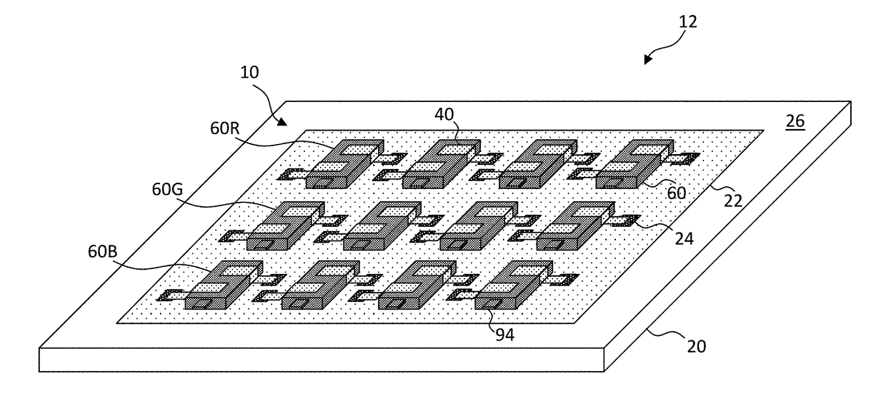
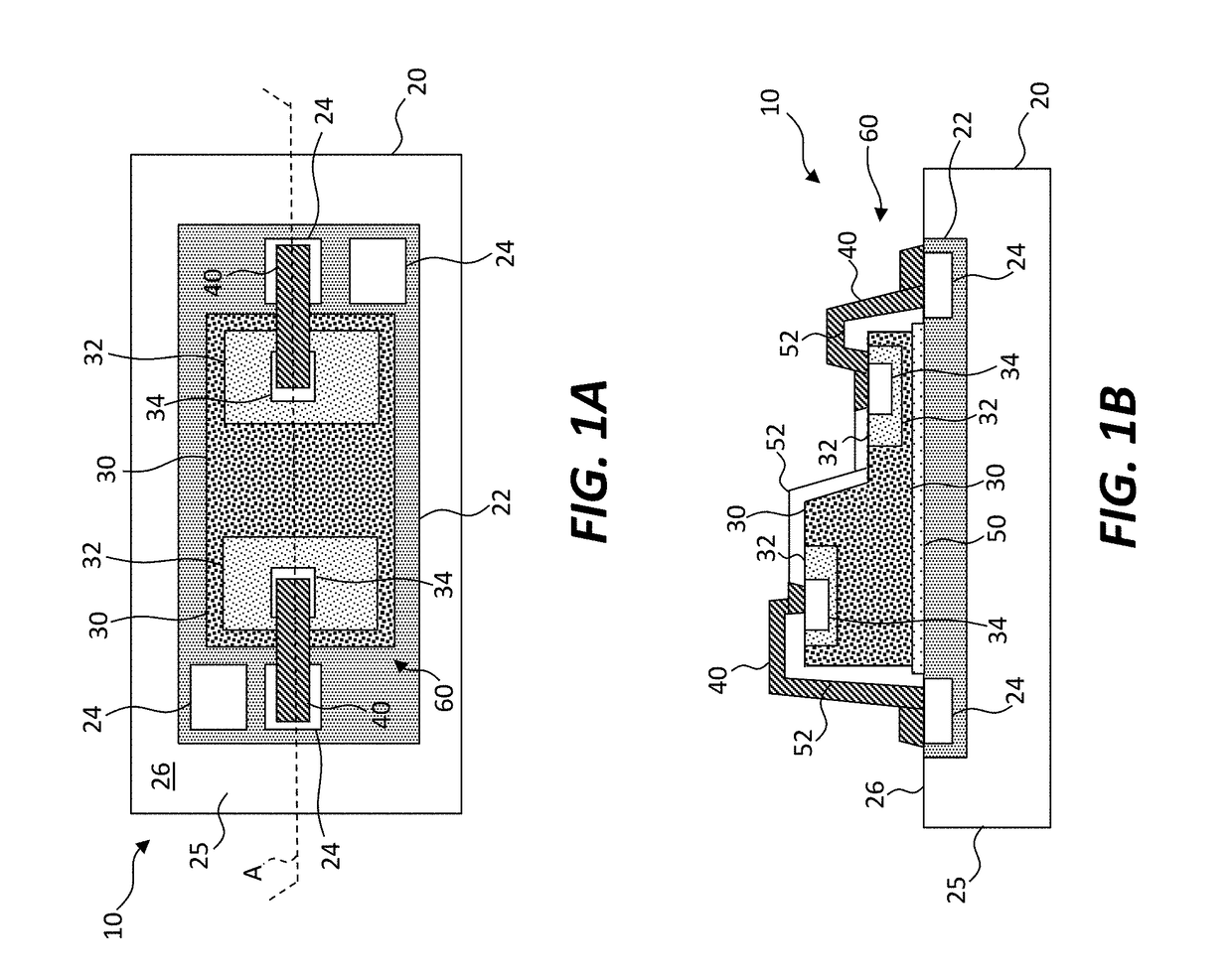
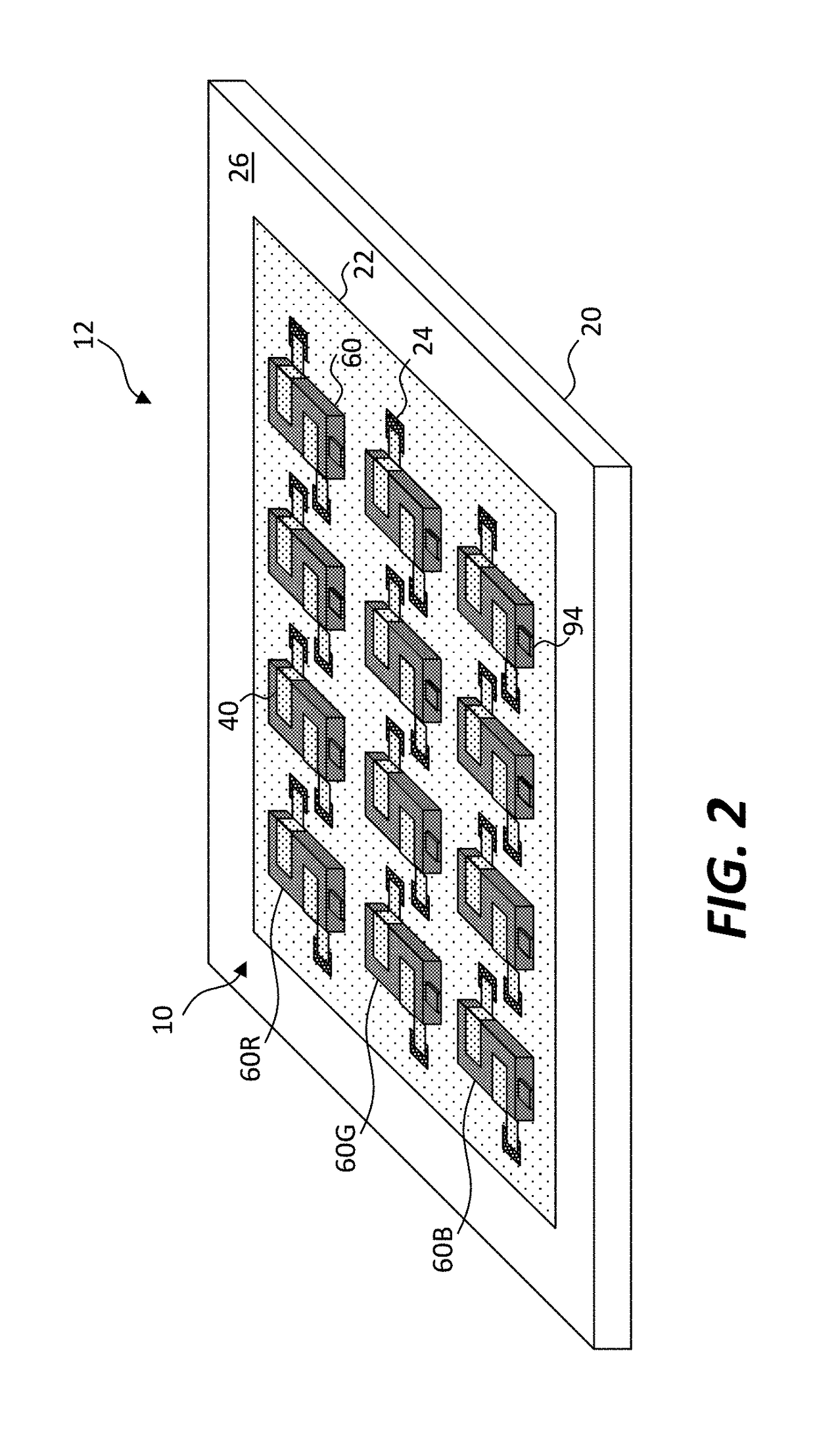
[0040]Referring to the schematic plan view of FIG. 1A, the schematic cross section of FIG. 1B taken across cross section line A of FIG. 1A, and the perspective of FIG. 2, in an embodiment of the present invention, a compound LED device 10 includes a semiconductor substrate 20. The semiconductor substrate 20 can be a silicon substrate. The semiconductor substrate 20 includes an active electronic circuit 22, for example a...


PUM


Abstract

A compound light-emitting diode (LED) device includes a semiconductor substrate having an active electronic circuit formed in or on the semiconductor substrate. Two or more electrically conductive circuit connection pads are formed in or on the semiconductor substrate and are electrically connected to the active electronic circuit. One or more micro-transfer printed LEDs each have at least two LED electrodes or connection pads and a fractured LED tether. An adhesive layer is disposed between the semiconductor substrate and each LED to adhere the semiconductor substrate to the LED. Two or more electrical conductors electrically connect one of the electrodes or LED connection pads to one of the circuit connection pads.

Description

PRIORITY APPLICATION[0001]This application claims priority to and benefit of U.S. Patent Application No. 62 / 344,148, filed Jun. 1, 2016, entitled Micro-Transfer-Printed Light-Emitting Diode Device, the content of which is hereby incorporated by reference in its entirety.FIELD OF THE INVENTION[0002]The present invention relates to integrated heterogeneous structures, and more particularly to light-emitting diode micro-devices, including displays.BACKGROUND OF THE INVENTION[0003]Micro-displays are small displays, typically having a display diameter of only a few centimeters intended for viewing by only one person at a time. Often, micro-displays are found in head-mounted virtual reality or augmented reality systems and include a separate micro-display mounted in front of each of a viewer's eyes. Typical micro-display systems include projected or direct-view displays based on liquid crystal or organic light-emitting diode devices.[0004]Micro-displays are typically near-to-eye displays ...

Claims


Application Information

Patent Timeline
IPC IPC(8): H01L25/075H01L25/16H01L33/62H01L33/60H01L27/12
CPCH01L25/0753H01L33/62H01L33/60H01L27/1214H01L2933/0033H01L2933/0066H01L25/167H01L2224/18
Inventor BOWER, CHRISTOPHERCOK, RONALD S.
Owner X DISPLAY CO TECH LTD
Why Eureka
Try Eureka