Organic light emitting diode device, display panel and display device

A technology of light-emitting diodes and devices, which is applied in the fields of electric solid-state devices, semiconductor devices, and semiconductor/solid-state device manufacturing, etc., can solve the problems of high potential barrier and high device driving voltage

Active Publication Date: 2015-06-10
BOE TECH GRP CO LTD
View PDF5 Cites 13 Cited by
  • Summary
  • Abstract
  • Description
  • Claims
  • Application Information

AI Technical Summary

Problems solved by technology

[0005] The embodiments of the present invention provide an organic electroluminescent device, a display panel, and a display device, which are used to solve the proble...

Method used


Image

  • Organic light emitting diode device, display panel and display device
  • Organic light emitting diode device, display panel and display device
  • Organic light emitting diode device, display panel and display device

Examples


Embodiment Construction

[0034] In order to make the purpose, technical solutions and advantages of the present invention clearer, the present invention will be further described in detail below in conjunction with the accompanying drawings. Obviously, the described embodiments are only some of the embodiments of the present invention, rather than all of them. Based on the embodiments of the present invention, all other embodiments obtained by persons of ordinary skill in the art without making creative efforts belong to the protection scope of the present invention.

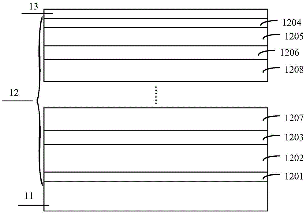
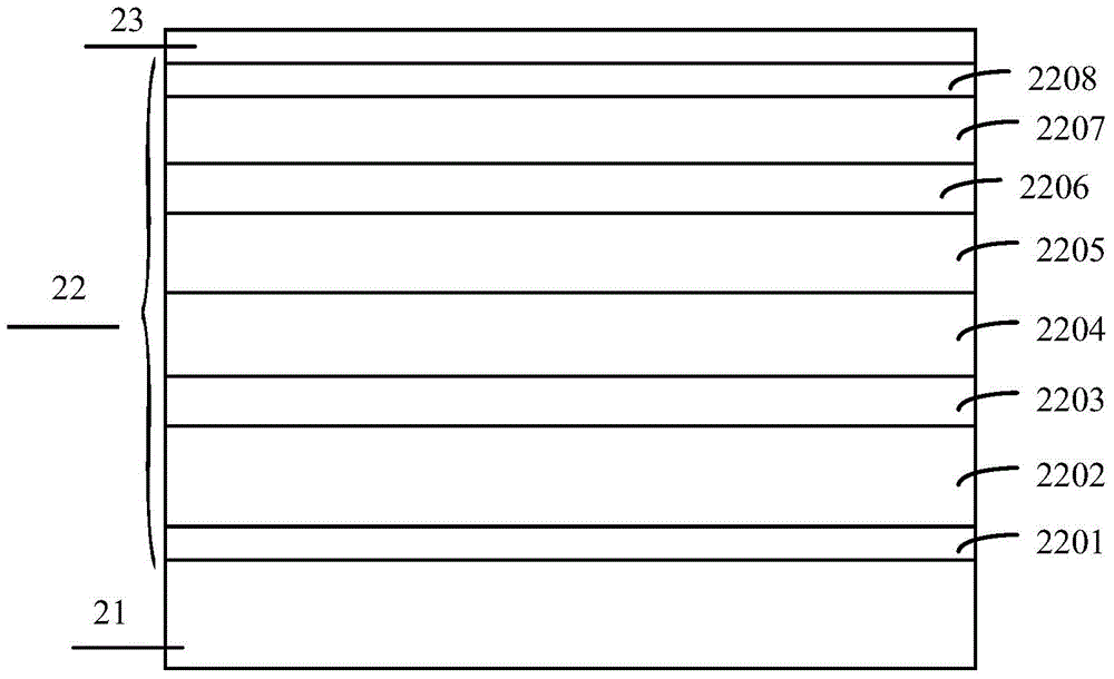
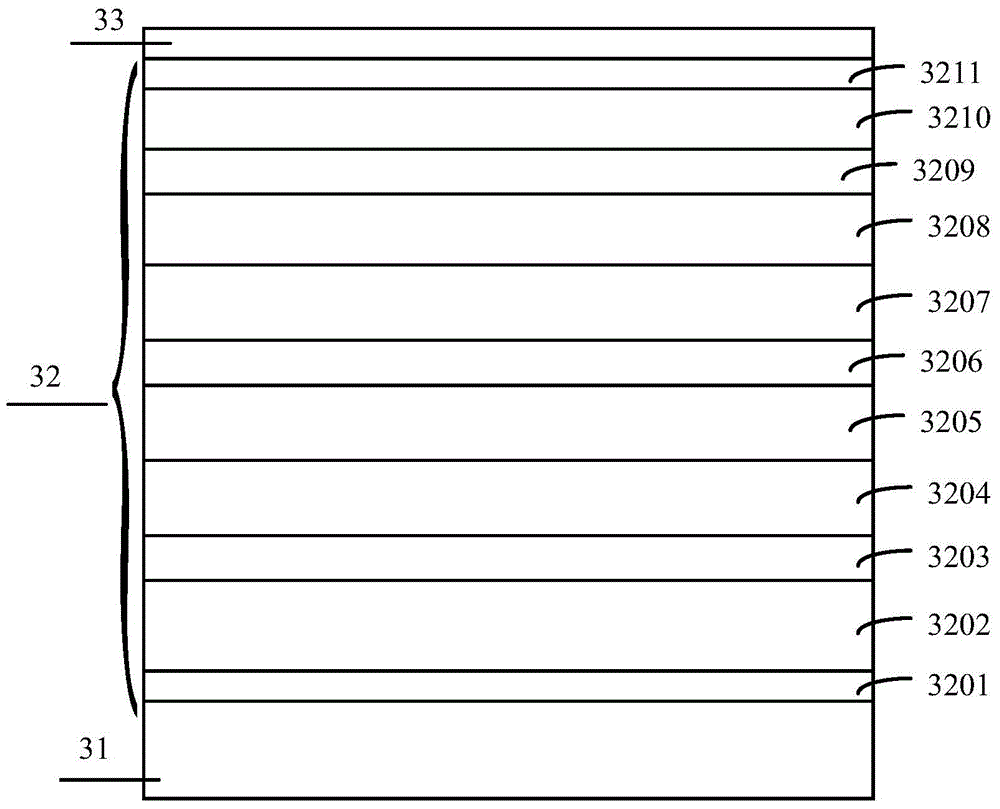
[0035] In the embodiment of the present invention, by improving the existing tandem top-emitting OLED devices, using a homojunction structure and improving the functional layers of the top-emitting OLED devices connected in series, the functional layers include: A hole injection layer, a hole transport layer, and a hole-side light-emitting layer arranged in sequence near the anode side, an electron injection layer, an electron-transport ...


PUM


Abstract

The invention discloses an organic light emitting diode device, a display panel and a display device. The organic light emitting diode device is mainly characterized in that existing serial top-emitting OLED devices are improved, a homojunction structure is utilized and functional layers of the top-emitting OLED devices connected in series are improved, so that each function layer comprises a hole injection layer, a hole transmission layer, a hole side light-emitting layer, an electron injection layer, an electron transmission layer, an electron side light-emitting layer and at least one group of charge producing layers a and charge producing layers b located between the hole side light-emitting layer and the electron side light-emitting layer, the hole injection layer, the hole transmission layer and the hole side light-emitting layer are sequentially arranged on the side close to an anode, the electron injection layer, the electron transmission layer and the electron side light-emitting layer are sequentially arranged on the side close to a cathode. A first light-emitting unit ...and an Nth light-emitting unit of each serial top-emitting OLED device are of homojunction structures, the using categories of organic materials are decreased, injection potential barriers of charge carriers in the devices are eliminated, the charge carrier injection efficiency and the efficiency of the devices are improved, and drive voltage of the devices is reduced.

Description

technical field [0001] The invention relates to the field of display technology, in particular to an organic light emitting diode device, a display panel, and a display device. Background technique [0002] Organic Light-Emitting Diode (OLED) has the characteristics of low energy consumption, low driving voltage, wide color gamut, simple manufacturing process, wide viewing angle, and fast response. International research hotspot in recent years. [0003] The tandem OLED that has been widely studied contains multiple light-emitting units, and the multiple light-emitting units are connected with a charge generation layer. The light emission does not affect each other, and the current density in the device is low, which can effectively avoid the effect of excess current. The resulting thermal quenching effect further improves the current efficiency, brightness, and lifetime of the OLED. By doping luminescent materials with different emission wavelengths, each light-emitting u...

Claims


Application Information

Patent Timeline
IPC IPC(8): H01L51/50
CPCH10K85/211H10K85/623H10K85/654H10K85/342H10K85/6572H10K30/865H10K50/131H10K50/11H10K50/15H10K50/16H10K50/17H10K50/19H10K50/82H10K50/171H10K50/818H10K85/60H10K85/311H10K2101/80H10K2102/00H10K2102/103H10K2102/3026
Inventor 毕文涛李娜梁逸南
Owner BOE TECH GRP CO LTD
Why Eureka
Try Eureka