A method for preparing a three-dimensional gate-around structure semiconductor field effect transistor device

A technology of field-effect transistors and semiconductors, applied in semiconductor devices, semiconductor/solid-state device manufacturing, electrical components, etc., to achieve high designability, high flexibility, and less time-consuming effects

CN105304501BActive Publication Date: 2019-08-23INST OF PHYSICS - CHINESE ACAD OF SCI
3 Cites 0 Cited by

Patent Information

Authority / Receiving Office
CN · China
Patent Type
Patents(China)
Current Assignee / Owner
Publication Date
2019-08-23

Smart Images

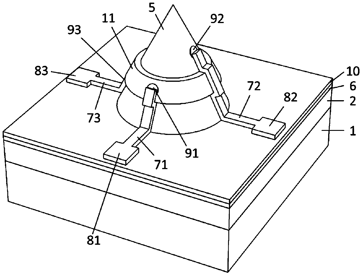
  • Figure 1
    Figure 1
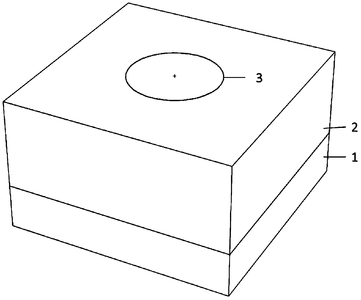
  • Figure 2
    Figure 2
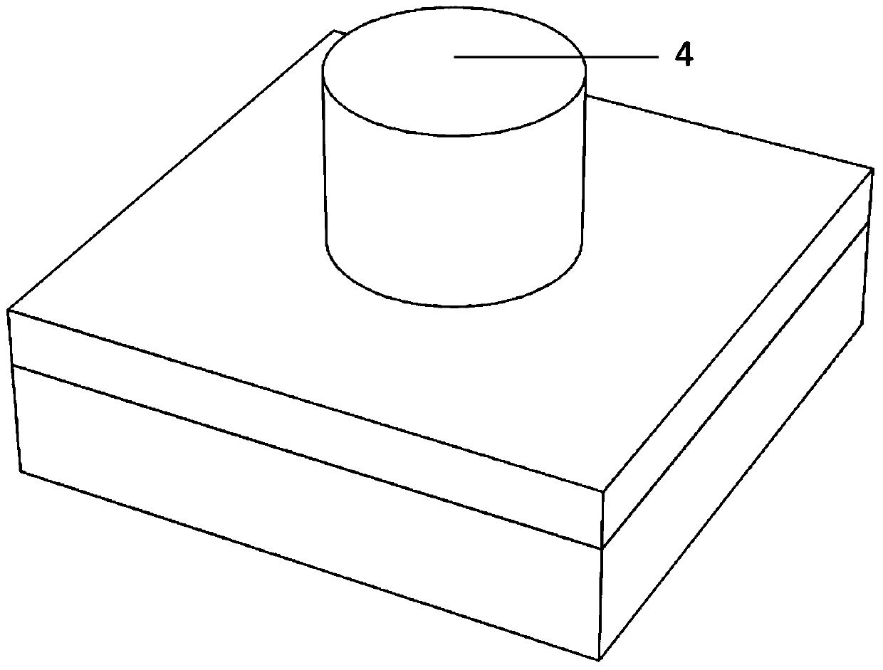
  • Figure 3
    Figure 3
Patent Text Reader

Abstract

The present invention provides a preparation method of a semiconductor field effect transistor device with a three-dimensional gate-all-around structure. A self-support three-dimensional micro-nano functional structure is taken as a carrier, and a micro-nano processing technology is employed to prepare the semiconductor field effect transistor device with the three-dimensional gate-all-around structure. The preparation method provided by the invention specifically comprises the following steps: a first dielectric layer is prepared on the surface of the self-support three-dimensional micro-nano functional structure; a three-dimensional gate-all-around metal electrode is prepared on the first dielectric layer; a second dielectric layer is prepared on the three-dimensional gate-all-around metal electrode to ensure electrical isolation of metal leads of a source electrode and a drain electrode and a grid; an electrode contact hole is prepared through etching on the second dielectric layer; and an electrode contact block is prepared and is connected with the electrode contact hole. The transistor device prepared by the method provided by the invention has effective grid-control characteristic, is able to isotropically regulate the field effect between a source electrode and a drain electrode and restrain a wall and corner effect; and moreover, a long and wide channel and smaller drain terminal parasitic capacitance are provided in the micro-nano grade so that the electric field diffusion of the drain terminal is reduced and the performance of the transistor device may be improved.
Need to check novelty before this filing date? Find Prior Art

Description

technical field

[0001] The invention relates to the technical field of semiconductors, in particular to a method for preparing a three-dimensional gate-around-structure semiconductor field-effect transistor device. Background technique

[0002] With the further development of electronic integration technology, the demand for miniaturization and high efficiency of electronic devices is gradually increasing. However, as the size of semiconductor devices continues to shrink, the method of improving device performance by proportionally reducing device size is approaching the limit. The channel effect and subthreshold performance degradation also limit the further reduction of device size, so more and more researchers pay attention to the use of transistors with complex geometric gate structures to increase the current control of the gate to the transistor channel. Among all the multi-gate structures proposed so far, the ring gate has the advantages of better chip area reduction,...

Examples

Embodiment Construction

[0040] figure 1 A schematic structural diagram of a three-dimensional gate-around semiconductor field effect transistor device according to an embodiment of the present invention is shown. Its preparation process specifically includes the following steps:

[0041] figure 2 It is a schematic diagram of the processing of the planar mask pattern according to an embodiment of the present invention, refer to figure 2 , firstly, the Si substrate 1 can be selected as the supporting substrate for the growth of the functional thin film layer, which is used for the preparation of the functional bulk material 2 on the substrate. The functional block material 2 can be selected from semiconductor materials, metal materials or electrical insulating materials. Among them, the Si substrate 1 needs to be cleaned and treated, specifically as follows: firstly, the Si substrate 1 is ultrasonically treated with acetone, ethanol, and deionized water; then the Si substrate 1 is blown dry with n...