Production method of three-dimensional ring gating semiconductor field effect transistor

A field-effect transistor and semiconductor technology, which is used in the manufacture of semiconductor/solid-state devices, semiconductor devices, electrical components, etc., to achieve the effect of suppressing corner effects, improving performance, and reducing time-consuming

Active Publication Date: 2017-05-17
INST OF PHYSICS - CHINESE ACAD OF SCI
View PDF3 Cites 1 Cited by
  • Summary
  • Abstract
  • Description
  • Claims
  • Application Information

AI Technical Summary

Problems solved by technology

[0003] However, the technology used in the currently reported three-dimensional gate-all-around transistor structure is still based on traditional micro-nano-fabrication semiconductor technology

Method used


Image

  • Production method of three-dimensional ring gating semiconductor field effect transistor
  • Production method of three-dimensional ring gating semiconductor field effect transistor
  • Production method of three-dimensional ring gating semiconductor field effect transistor

Examples


Embodiment Construction

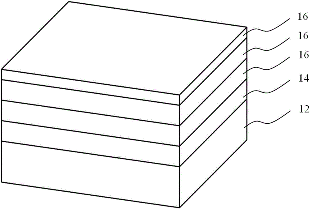
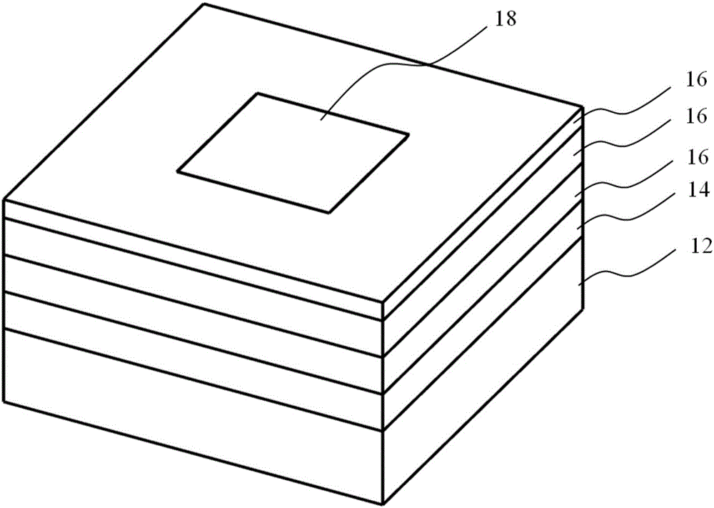
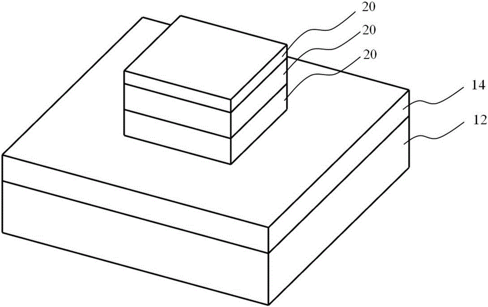
[0041] Figure 10 A schematic structural diagram of a three-dimensional gate-all-around semiconductor field effect transistor according to an embodiment of the present invention is shown. The preparation process specifically includes the preparation steps of the electrical insulation layer 14 and the functional structure layer 16 . figure 1 is a schematic diagram of preparing an electrical insulating layer 14 and a functional structural layer 16 on a substrate 12 according to an embodiment of the present invention. refer to figure 1, a silicon substrate can be selected as the supporting base 12 for the growth of the electrical insulating layer 14 and the functional structure layer 16 . The electrical insulating layer 14 can be selected from electrical insulating materials, such as silicon dioxide, undoped diamond, and the like. On the surface of the electrical insulation layer 14, one or more layers of functional structure layers 16 with different doping levels are grown. ...


PUM


Abstract

The invention provides a production method of a three-dimensional ring gating semiconductor field effect transistor, and belongs to the technical field of three-dimensional micro-nano structures. The method comprises the following steps of providing a substrate, forming an electric insulation layer on the substrate, and forming a functional structure later on the electric insulation layer; forming an active area in the electric insulation layer, and acquiring a self-support functional structure layer in the active area; forming an isolation layer in the other areas except the self-support functional structure layer, and forming a dielectric layer on the self-support functional structure layer and the isolation layer; applying metal material on the surface with the self-support functional structure layer to form a three-dimensional ring gating metal electrode; forming an electrode contact hole in the self-support functional structure layer and/or the three-dimensional ring gating metal electrode by etching; and forming an electrode contact block at the active area and/or the electric insulation layer, and forming a lead between the electrode contact block and the electrode contact hole to communicate the same. The method provided by the invention is less in consumed time, and high in yield, flexibility and designability.

Description

technical field [0001] The invention relates to the technical field of three-dimensional micro-nano devices, in particular to a preparation method of a three-dimensional gate-around semiconductor field effect transistor. Background technique [0002] At present, semiconductor integration technology is still full of challenges, and the demand for high integration and high performance is gradually increasing. As we all know, as the size of semiconductor devices continues to shrink, the method of improving device performance by scaling down the device size is approaching the limit, and the short-channel effect and subthreshold performance degradation also limit the further reduction of the device size. Therefore, more and more researchers use transistors with complex geometrical gate structures and ingenious processes to achieve high integration and high performance of devices. Among all the multi-gate structures proposed so far, the ring-shaped gate has the advantages of high...

Claims


Application Information

Patent Timeline
Patent Type & Authority Applications(China)
IPC IPC(8): H01L29/775H01L21/335H01L21/28H01L29/423
CPCH01L21/28008H01L29/42316H01L29/42376H01L29/66439H01L29/775
Inventor 顾长志郝婷婷李无瑕李俊杰
Owner INST OF PHYSICS - CHINESE ACAD OF SCI
Why Eureka
Try Eureka