Pixel structure, manufacturing method thereof and display panel

A technology of pixel structure and sub-pixel, applied in the direction of organic semiconductor devices, semiconductor devices, electrical components, etc., can solve the problems of color crosstalk and reduce the display quality of OLED display devices, and achieve the effect of alleviating color crosstalk and improving display quality.

Active Publication Date: 2016-03-23
TIANMA MICRO ELECTRONICS CO LTD +1
View PDF9 Cites 19 Cited by
  • Summary
  • Abstract
  • Description
  • Claims
  • Application Information

AI Technical Summary

Problems solved by technology

[0004] However, when the above-mentioned OLED display device performs pure color display, there is a color crosstalk phenomenon, that is, when the OLED display device displays a pure red picture, there is not only red in the display picture, but also some sub-pixels adjacent to the red sub-pixel. The color of the pixels, such as green or blue, reduces the display quality of the OLED display device

Method used


Image

  • Pixel structure, manufacturing method thereof and display panel
  • Pixel structure, manufacturing method thereof and display panel
  • Pixel structure, manufacturing method thereof and display panel

Examples


Embodiment Construction

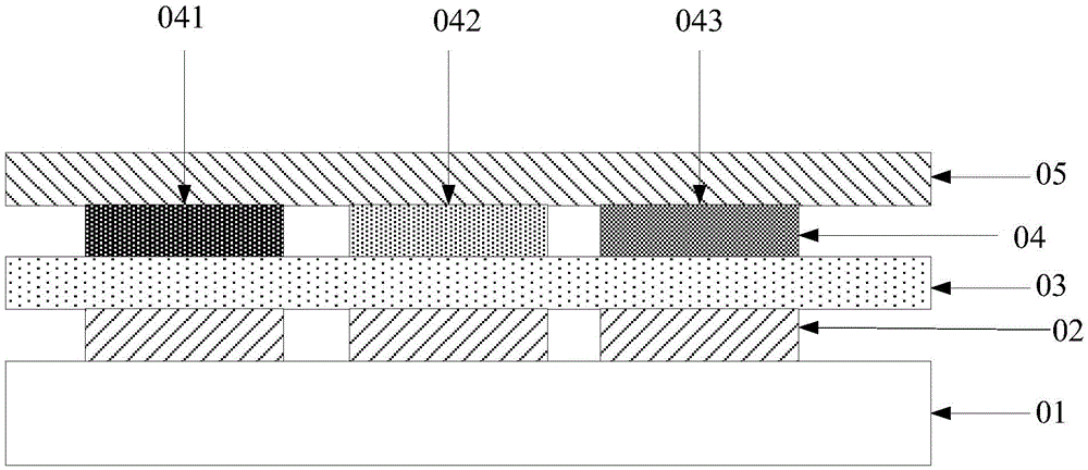
[0043] As mentioned in the background technology section, when the OLED display device in the prior art performs pure color display, there is a phenomenon of color crosstalk, that is, when the OLED display device displays a pure red picture, there is not only red in the display picture, but also some The color of the sub-pixels adjacent to the red sub-pixel, such as green or blue, reduces the display quality of the OLED display device.

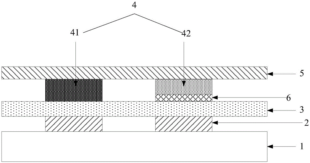
[0044] The inventor found through research that this is because the auxiliary light-emitting layer 03 corresponding to each light-emitting part in the light-emitting layer is a whole auxiliary light-emitting layer. When the red sub-pixel displays and the green sub-pixel does not display, it is located in the red The holes in the area of ​​the auxiliary light emitting layer 03 under the light emitting part 041 will be transported along the auxiliary light emitting layer 03 to the area of ​​the auxiliary light emitting layer 03 under the green li...


PUM


Abstract

The embodiment of the invention discloses a pixel structure, a manufacturing method thereof, and a display panel. The pixel structure includes a substrate, an anode layer, a first auxiliary light-emitting layer, a light-emitting layer, a cathode layer and at least one first resistor structure; the light-emitting layer at least comprises a first light-emitting portion and a second light-emitting portion; the first light-emitting portion corresponding to first sub pixels; the second light-emitting portion is corresponding to the second sub pixels; the turn-on voltage of the first sub pixels is larger than the turn-on voltage of the second pixels; the first resistor structures are located on a closed path from the first auxiliary light emitting layer to the cathode layer and are arranged at the vertical direction of the second light-emitting portion and are at least partially overlapped with the second light-emitting portion, and are not overlapped with the first light-emitting portion; and the absolute value of the difference value between the sum of the resistance values of the at least one first resistor structure and the second light-emitting portion and the resistance value of the first light-emitting portion is smaller than a first preset value, so that color crosstalk which occurs when a display panel comprising the pixel structure performs display can be alleviated, and the display quality of the display panel is improved.

Description

technical field [0001] The present invention relates to the field of display technology, in particular to a pixel structure and a manufacturing method thereof, and a display panel including the pixel structure. Background technique [0002] At present, OLED (Organic Light Emitting Diode) display devices usually include a plurality of sub-pixels, and adjacent sub-pixels emit light in different colors. For example, OLED display devices in the prior art include a plurality of periodically arranged red sub-pixels, green sub-pixels and blue sub-pixels to achieve different color display. [0003] Such as figure 1 As shown, the OLED display device in the prior art generally includes: a substrate 01: an anode layer 02 located on the surface of the substrate 01, the anode layer 02 is composed of a plurality of anode parts; 02 and the auxiliary light-emitting layer 03 of the substrate 01; the light-emitting layer 04 located on the surface of the auxiliary light-emitting layer 03, th...

Claims


Application Information

Patent Timeline
Patent Type & Authority Applications(China)
IPC IPC(8): H01L27/32
CPCH10K59/00H10K59/35H10K59/121H10K50/00H10K50/13H10K50/814H10K50/824H10K71/00H10K71/166H10K2102/00H10K2102/351
Inventor 熊志勇范刘静
Owner TIANMA MICRO ELECTRONICS CO LTD
Why Eureka
Try Eureka