The printed circuit board and the method for manufacturing the same

A technology for printed circuit boards and circuit patterns, applied in the fields of printed circuit manufacturing, printed circuits, printed circuits, etc., can solve problems such as design limitations, and achieve the effects of increasing conductivity, increasing installation area, and reducing resistance

Active Publication Date: 2017-01-25
LG INNOTEK CO LTD
View PDF4 Cites 0 Cited by
  • Summary
  • Abstract
  • Description
  • Claims
  • Application Information

AI Technical Summary

Problems solved by technology

[0015] However, when this additional seed layer is formed so that plating is performed even for surface treatment of PCBs that are generally performed by electroless plating, there may be design limitations.

Method used


Image

  • The printed circuit board and the method for manufacturing the same
  • The printed circuit board and the method for manufacturing the same
  • The printed circuit board and the method for manufacturing the same

Examples


Embodiment Construction

[0055] Hereinafter, embodiments of the present disclosure will be described in detail with reference to the accompanying drawings so that those skilled in the art can easily repeat using the embodiments. However, the embodiments may be variously modified, and the present disclosure is not limited thereto.

[0056] In the following description, when a predetermined part "includes" a predetermined element, the predetermined part does not exclude other elements, but may also include other components, unless otherwise specified.

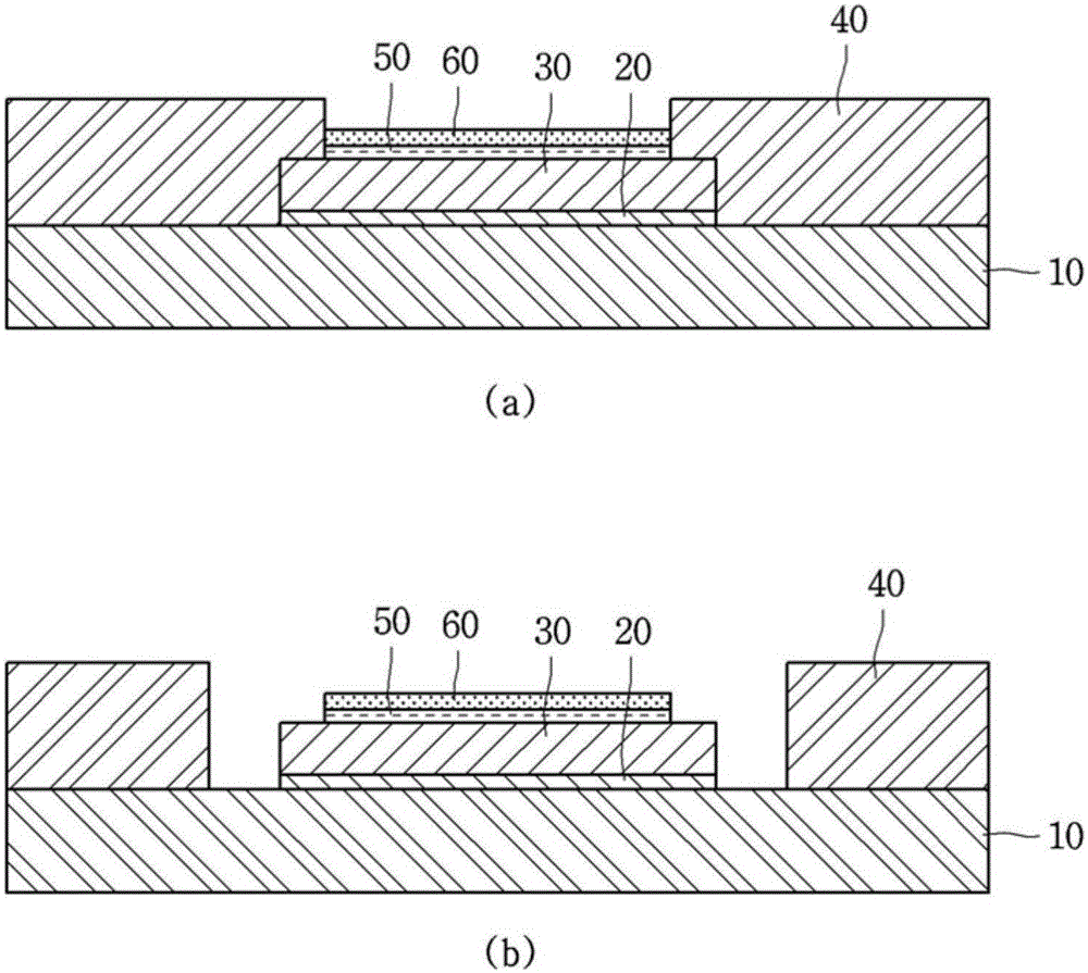
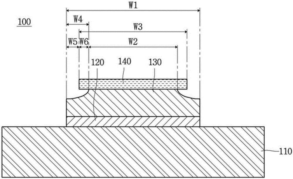
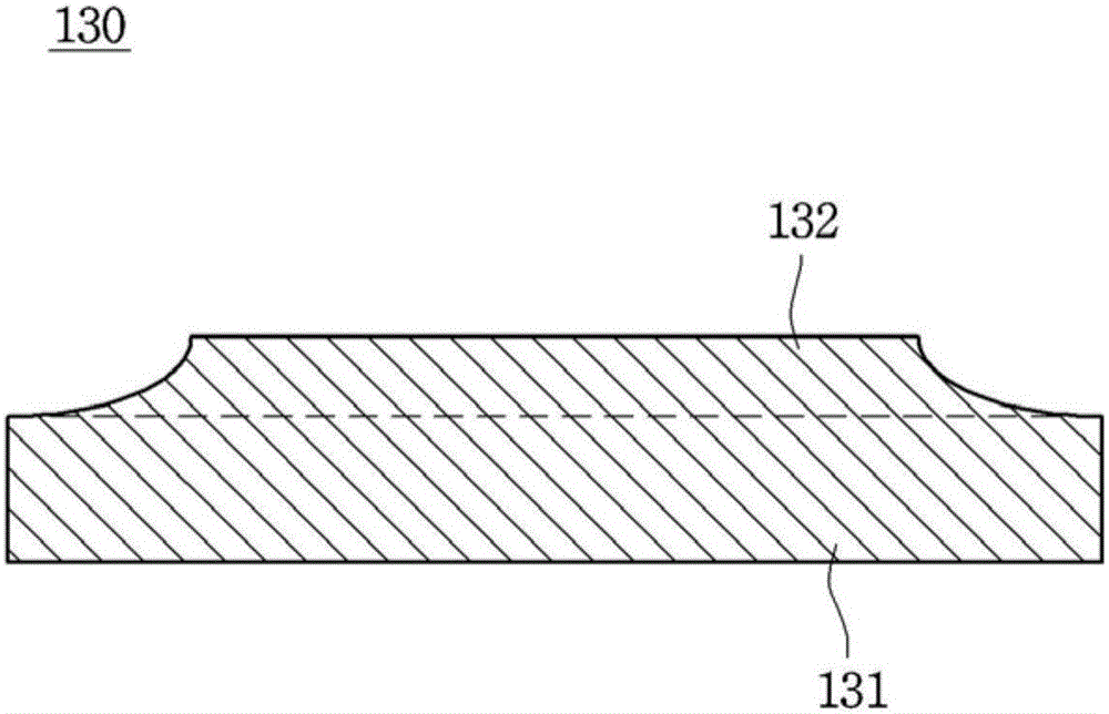
[0057] The thicknesses and sizes of layers shown in the drawings may be exaggerated, omitted, or schematically drawn for the purpose of convenience or clarity. In addition, the size of elements may not utterly reflect an actual size. Throughout the drawings, like reference numerals will assign like elements.

[0058] In the description of an embodiment, it will be understood that when a layer, film, region or panel is referred to as being "on" another ...


PUM


Abstract

A printed circuit board includes an insulating layer, a circuit pattern on the insulating layer, and a surface treatment layer on the circuit pattern. The surface treatment layer includes a bottom surface having a width wider than a width of a top surface of the circuit pattern.

Description

[0001] CROSS-REFERENCE TO RELATED APPLICATIONS [0002] This application claims priority under 35 U.S.C. 119 and 35 U.S.C. 365 to Korean Patent Application No. 10-2015-0100404 (filed on July 15, 2015), which is hereby incorporated by reference in its entirety enter. technical field [0003] The present disclosure relates to a printed circuit board, and more particularly, to a printed circuit board including: a circuit pattern having a curved surface in a part of its side; and, a surface formed by electroplating, and a manufacturing method thereof processing layer. Background technique [0004] A printed circuit board (PCB) formed by printing a circuit wiring pattern on an electrically insulating substrate using a conductive material such as copper (Cu) means a board on which electronic components are closely mounted. That is, the PCB means a circuit board in which the mounting positions of electronic components are determined, and circuit patterns are printed on and fixed ...

Claims


Application Information

Patent Timeline
Patent Type & Authority Applications(China)
IPC IPC(8): H05K3/24
CPCH05K3/24H05K2201/0364H05K2201/098H05K3/108H05K2201/0338H05K2201/0989H05K2201/099H05K2203/1184H05K3/244H05K3/188H05K3/181H05K1/0296C25D3/48C25D5/022C25D5/48C25D7/123H05K1/09H05K1/11C25D3/38
Inventor 裵允美权纯圭金相和李相永李珍鹤李汉洙郑东宪丁仁晧崔大荣黄贞镐
Owner LG INNOTEK CO LTD
Why Eureka
Try Eureka