Manufacturing method and PCB of groove bottom pattern stepped groove

A manufacturing method and technology of stepped grooves, which are applied in multilayer circuit manufacturing, printed circuit manufacturing, printed circuit and other directions, can solve the problems of complex process, many structural design restrictions, and difficult manufacturing, so as to reduce the difficulty of operation and improve work efficiency. , The effect of the simple process

Active Publication Date: 2020-01-17
DONGGUAN SHENGYI ELECTRONICS
View PDF6 Cites 0 Cited by
  • Summary
  • Abstract
  • Description
  • Claims
  • Application Information

AI Technical Summary

Problems solved by technology

This method has the following problems: for the non-metallized stepped groove on the side wall, due to the pre-made graphics, the motherboard must protect the graphics in the stepped groove, which has many restrictions on the structural design, the production is difficult, and the process is complicated, which restricts the design of the stepped groove graphic board. Promote application

Method used


Image

  • Manufacturing method and PCB of groove bottom pattern stepped groove
  • Manufacturing method and PCB of groove bottom pattern stepped groove
  • Manufacturing method and PCB of groove bottom pattern stepped groove

Examples


Embodiment 1

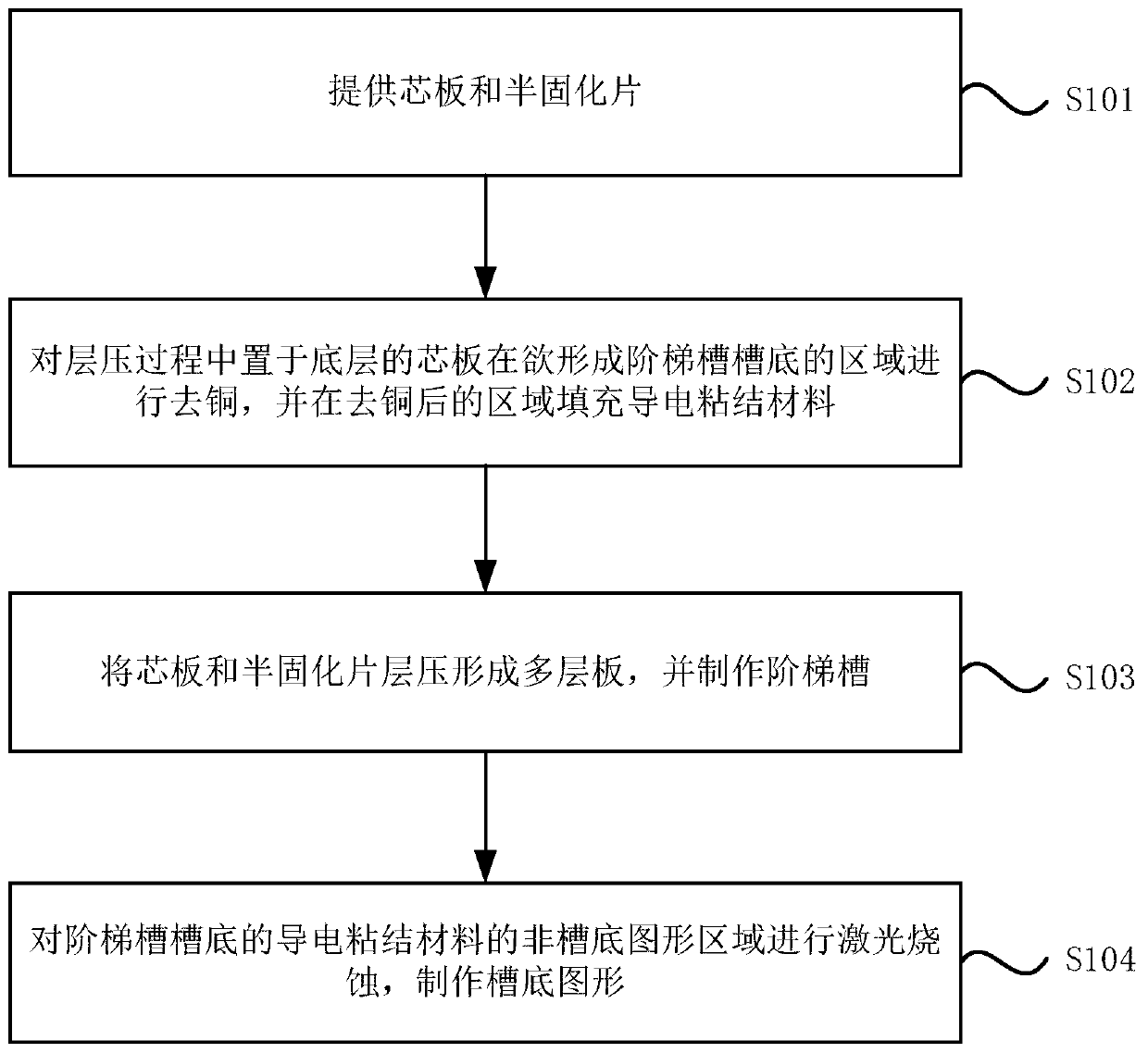
[0034] see figure 1 , the present embodiment 1 provides a method for manufacturing a stepped groove with a groove bottom pattern, comprising the steps of:

[0035] S101. Provide core board and prepreg.

[0036] S102, remove copper in the area where the bottom of the stepped groove is to be formed on the core board placed on the bottom layer during the lamination process, and fill the area after the copper removal with conductive bonding material, such as figure 2 shown.

[0037] Wherein, the composition of the conductive bonding material includes but not limited to resin matrix, conductive particles, dispersion additives and auxiliary agents, commonly used matrix is ​​generally thermosetting adhesive such as epoxy resin, silicone resin, polyimide resin , phenolic resin, polyurethane, acrylic resin and other adhesive systems. After curing, these adhesives form the molecular skeleton structure of conductive bonding materials, provide mechanical properties and bonding perform...

Embodiment 2

[0057] The second embodiment provides a PCB, including a stepped groove with a groove bottom pattern, and the stepped groove is manufactured according to the manufacturing method provided in the first embodiment.


PUM


Abstract

The embodiment of the invention discloses a method for manufacturing a step groove of a groove bottom pattern and a PCB. The method comprises the following steps: providing a core board and a prepreg;Removing copper from the core plate placed in the bottom layer in the laminating process in the area where the bottom of the step groove is to be formed, and filling the area after removing copper with conductive adhesive material; Laminating the core plate and the prepreg sheet to form a multilayer plate, and manufacturing a step groove; Laser ablation is carried out on the non-groove bottom pattern area of the conductive adhesive material at the bottom of the step groove to produce the groove bottom pattern. Compared with the prior art, the invention has no design limitation, the process method is simpler, no special equipment or special process is needed, the operation difficulty is reduced, the work efficiency is improved, and the invention is suitable for mass production.

Description

technical field [0001] Embodiments of the present invention relate to the technical field of printed circuit boards, in particular to a method for manufacturing a stepped groove with a groove bottom pattern and a PCB. Background technique [0002] With the advancement of science and technology, electronic products have become indispensable daily necessities in people's lives, and PCB (Printed Circuit Board, printed circuit board) is an important part of electronic products. In recent years, people have more and more functional requirements for electronic products. The more it is, the higher the requirements are for the PCB. [0003] Due to its special structure and electrical properties, stepped grooves are widely used in three-dimensional three-dimensional assembly, reducing the assembly volume of electrical equipment, and special electrical properties. At present, there are various manufacturing methods for stepped groove circuit boards, but for The method of making the g...

Claims


Application Information

Patent Timeline
Patent Type & Authority Patents(China)
IPC IPC(8): H05K3/46
CPCH05K3/4611
Inventor 刘梦茹纪成光陈正清
Owner DONGGUAN SHENGYI ELECTRONICS
Why Eureka
Try Eureka