

A metamaterial wave-absorbing structure based on a magnetic wave-absorbing material and multiple layers of resistive films
A technology of magnetic wave absorption and resistive film, applied in the direction of magnetic/electric field shielding, electrical components, antennas, etc., to achieve good wave absorption effect, thin thickness, and high strength
- Summary
- Abstract
- Description
- Claims
- Application Information
AI Technical Summary
Problems solved by technology
Method used
Image

Examples
specific Embodiment
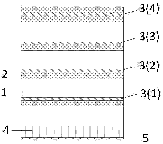
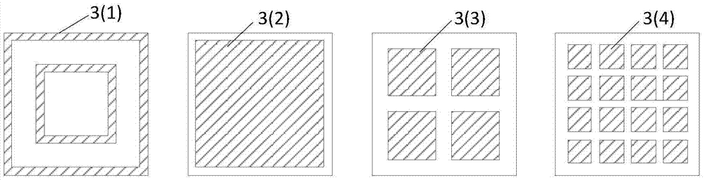
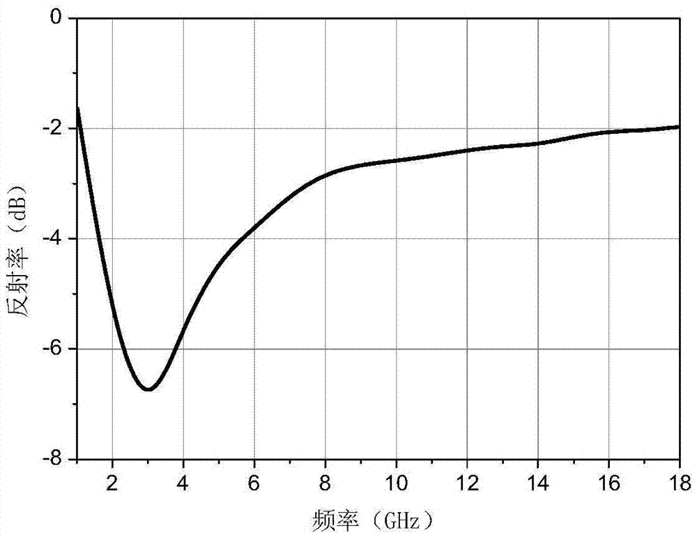
[0023] figure 1 The length and width of the metamaterial wave-absorbing structural unit shown in the figure are both 3.8mm, and the total thickness is about 6.5mm. Among them, the four layers of PMI foam 1 all use XK110 with a thickness of 1.2mm and a relative dielectric constant of 1.15; the thickness of the five layers of PET dielectric substrate 2 is 0.125mm, and the relative dielectric constant is 3.1; the resistance film 3 (1)-3 (4) The specific resistance film shape is as follows figure 2 As shown, the square resistance values of the resistive films 3(1)-3(4) are 150Ω, 220Ω, 350Ω and 60Ω in turn; the magnetic absorbing material is WAT_1mm with a thickness of 1mm, and its absorbing characteristics are as follows image 3 As shown, it can be seen that the main operating frequency band of the magnetic material is 1.5GHz-6GHz.
[0024] The reflectance curve of this embodiment is as Figure 4 shown by the solid line. Replace the magnetic material with PMI foam of the s...
PUM
 Abstract
Description
Claims
Application Information