A kind of LED chip and its manufacturing method

An LED chip and manufacturing method technology, applied in semiconductor devices, electrical components, circuits, etc., can solve problems such as uneven current spreading, and achieve the effects of solving uneven current spreading, improving uniformity, and uniform current spreading

Active Publication Date: 2019-10-18
XIAMEN CHANGELIGHT CO LTD
View PDF5 Cites 0 Cited by
  • Summary
  • Abstract
  • Description
  • Claims
  • Application Information

AI Technical Summary

Problems solved by technology

[0005] In order to solve the above problems, the technical solution of the present invention provides an LED chip and its manufacturing method, which solves the problem of uneven current diffusion in the LED chip and improves the uniformity of the LED chip's light emission.

Method used


Image

  • A kind of LED chip and its manufacturing method
  • A kind of LED chip and its manufacturing method
  • A kind of LED chip and its manufacturing method

Examples


Embodiment Construction

[0041] The technical solutions in the embodiments of the present invention will be clearly and completely described below in conjunction with the accompanying drawings in the embodiments of the present invention. Obviously, the described embodiments are only a part of the embodiments of the present invention, rather than all the embodiments. Based on the embodiments of the present invention, all other embodiments obtained by those of ordinary skill in the art without creative work shall fall within the protection scope of the present invention.

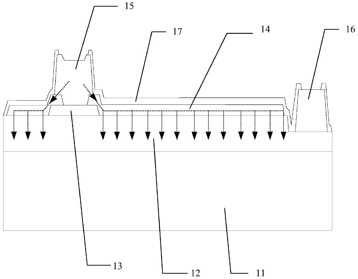
[0042] The conventional LED chip structure is as figure 1 As shown, figure 1 It is a schematic structural diagram of a conventional LED chip. The substrate 11 is provided with an epitaxial structure 12, and the epitaxial structure 12 has an N-type semiconductor layer, a quantum well light-emitting layer, and a P-type semiconductor layer arranged on the substrate 11 in sequence. A groove is provided on the epitaxial structure 12 to expose ...


PUM


Abstract

The invention discloses an LED chip and a manufacturing method thereof. The LED chip comprises: a substrate; an epitaxial structure arranged on the substrate, and the epitaxial structure includes an N-type semiconductor layer, a quantum well light-emitting layer and a P-type semiconductor layer arranged in sequence. The predetermined region of the epitaxial structure has a groove, and the groove is used to expose part of the N-type semiconductor layer; the P-type semiconductor layer has a first region, a second region and a third region; a first transparent conductive layer covering the first region; A current blocking layer covering the second region and part of the first transparent conductive layer; a second transparent conductive layer covering another part of the first transparent conductive layer, the third region and part of the current blocking layer; a P electrode covering another part of the current blocking layer; An N electrode arranged in the groove and electrically connected to the N-type semiconductor layer. The technical scheme of the invention solves the problem of uneven current diffusion in the LED chip, and improves the uniformity of light emission of the LED chip.

Description

Technical field [0001] The present invention relates to the technical field of semiconductor devices, and more specifically, to an LED chip and a manufacturing method thereof. Background technique [0002] The light-emitting principle of light-emitting diodes (LEDs) is to use the energy difference between electrons moving between N-type and P-type semiconductors to release energy in the form of light. This light-emitting principle is different from the light-emitting principle of incandescent lamps. Called cold light source. Because light-emitting diodes have the advantages of high durability, long life, light weight, and low power consumption, they are used in many fields such as signal indicators, lighting devices, and display devices. [0003] The common structure of an LED chip is to sequentially form an N-type semiconductor layer, a quantum well light-emitting layer, and a P-type semiconductor layer on a substrate. Part of the P-type semiconductor layer and the quantum well ...

Claims


Application Information

Patent Timeline
Patent Type & Authority Patents(China)
IPC IPC(8): H01L33/00H01L33/14H01L33/42
Inventor 刘英策刘兆宋彬吴奇隆李俊贤
Owner XIAMEN CHANGELIGHT CO LTD
Why Eureka
Try Eureka