Embedded type TSV adapter plate structure for numerous-layer wiring

A multi-layer wiring and adapter board technology, which is applied to semiconductor/solid-state device parts, semiconductor devices, electrical components, etc., can solve the problem of not being able to meet the development needs of high interconnection density of TSV adapter boards, and the difficulty of rewiring layers, etc. problem, to achieve the effect of compact structure and improved packaging yield

Active Publication Date: 2017-11-24
58TH RES INST OF CETC
View PDF3 Cites 14 Cited by
  • Summary
  • Abstract
  • Description
  • Claims
  • Application Information

AI Technical Summary

Problems solved by technology

However, the traditional RDL preparation technology is limited by the technological level, and it is very difficult to prepare multi-laye

Method used


Image

  • Embedded type TSV adapter plate structure for numerous-layer wiring
  • Embedded type TSV adapter plate structure for numerous-layer wiring
  • Embedded type TSV adapter plate structure for numerous-layer wiring

Examples


Example Embodiment

[0016] The present invention will be further described below with reference to the specific drawings and embodiments.

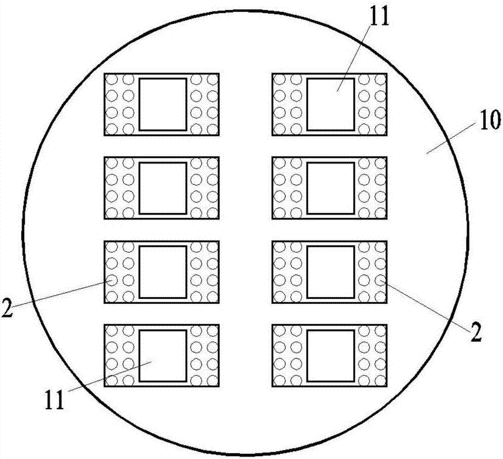
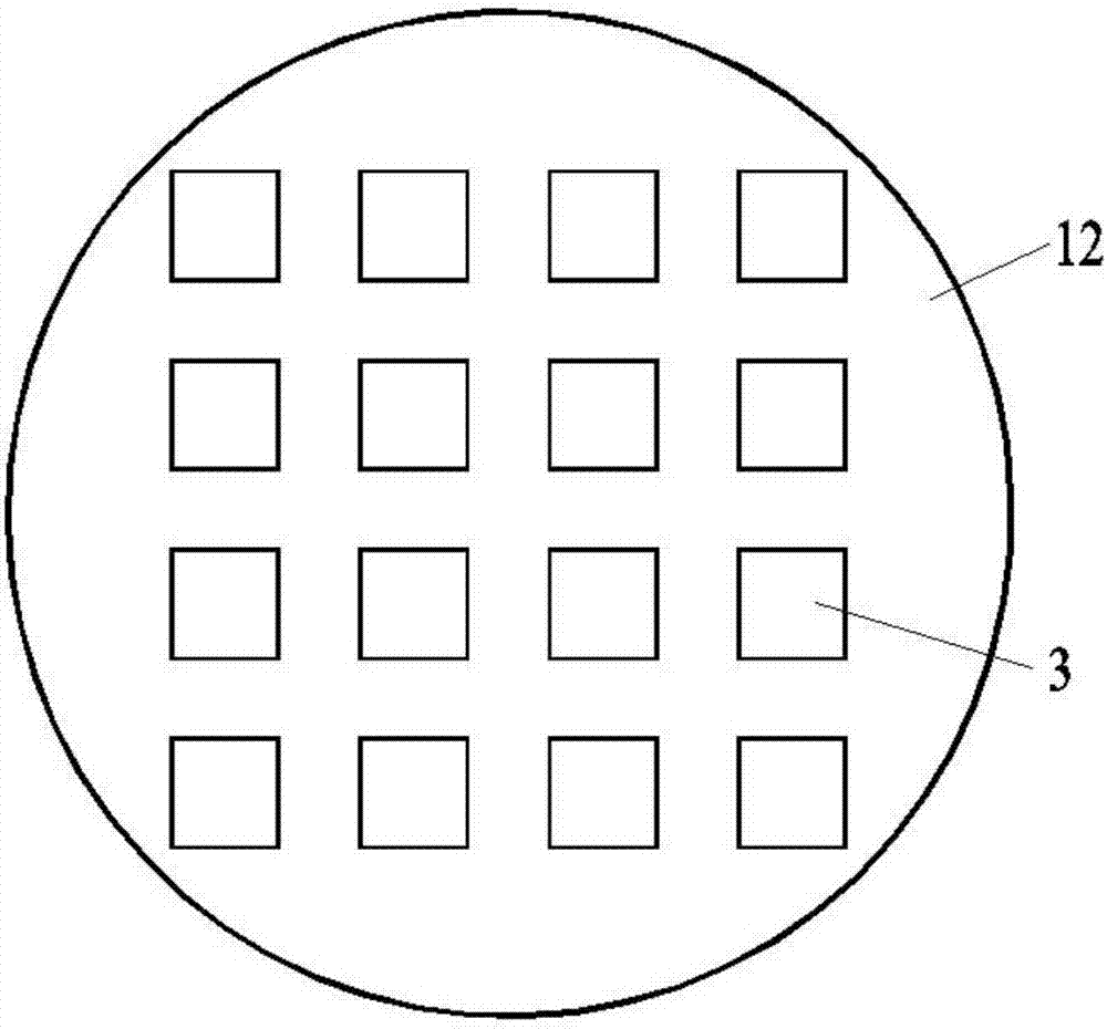
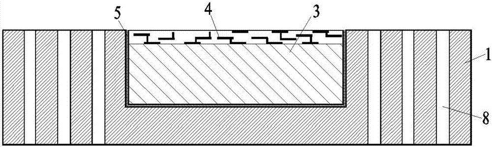
[0017] like Figure 5 As shown: in order to effectively increase the number of wiring layers and realize high-density chip level packaging and system packaging, the present invention includes an adapter board body 1; a wiring adapter board slot 11 is recessed in the adapter board body 1, A wiring adapter board 3 is arranged in the wiring adapter board slot 11, and a pole multilayer wiring 4 is arranged on the wiring adapter board 3. The wiring adapter board 3 is connected to the adapter board body through the pole multilayer wiring 4. 1. The rewiring layer 6 on the adapter board on the upper surface is electrically connected, and the rewiring layer 6 on the adapter board is connected to the lower surface of the adapter board body 1 through the filling connector 8 filled in the through hole 2 in the adapter board body 1. The rewiring layer 9 under the adapter...


PUM


Abstract

The invention relates to an adapter plate structure, in particular to an embedded type TSV adapter plate structure for numerous-layer wiring, which belongs to the technical field of integrated circuit packaging. According to the technical scheme provided by the invention, the embedded type TSV adapter plate structure for numerous-layer wiring comprises an adapter plate body, wherein a wiring adapter plate groove is formed in the adapter plate body in a concave manner, a wiring adapter plate is arranged in the wiring adapter plate groove, numerous-layer wires are arranged on the wiring adapter plate, the wiring adapter plate is electrically connected with an adapter plate upper redistribution layer on the upper surface of the adapter plate body by means of the numerous-layer wires, the adapter plate upper redistribution layer is electrically connected with an adapter plate lower redistribution layer on the lower surface of the adapter plate body by means of filling connectors filled in through vias of the adapter plate body, a plurality of solder balls are arranged on the adapter plate lower redistribution layer, and the solder balls are electrically connected with the adapter plate lower redistribution layer. The embedded type TSV adapter plate structure can effectively increase the number of wiring layers, realizes the high-density chip scale packaging and system packaging, and is safe and reliable.

Description

technical field [0001] The invention relates to an adapter board structure, in particular to an embedded TSV adapter board structure with extremely multi-layer wiring, and belongs to the technical field of integrated circuit packaging. Background technique [0002] With the development of electronic products in the direction of miniaturization, high performance, and high reliability, the degree of system integration is also increasing. In this case, the way to improve performance by further reducing the feature size of integrated circuits and the line width of interconnect lines is limited by the physical properties of materials and equipment technology, and it is difficult for the traditional Moore's Law to continue to develop. [0003] TSV (Through Silicon Via) technology enables vertical interconnection between chips and chips, chips and substrates, effectively shortening the information transmission path, and achieving more functions, higher power, and more terminals in ...

Claims


Application Information

Patent Timeline
IPC IPC(8): H01L23/498H01L21/48
CPCH01L23/49827H01L23/49861H01L21/4839H01L21/486H01L2224/73267H01L2224/92244H01L2924/15153H01L2224/04105H01L2224/19H01L2224/32225H01L2924/157H01L2924/15788
Inventor 明雪飞朱家昌
Owner 58TH RES INST OF CETC
Why Eureka
Try Eureka