Construction method for single-project and multiple-project compatible wafer diagram

A construction method and wafer map technology, applied in special data processing applications, instruments, electrical digital data processing, etc., can solve the problems of single wafer map construction method and complex multi-target wafer map construction method

Inactive Publication Date: 2018-01-12
苏州伊欧陆系统集成有限公司
View PDF5 Cites 6 Cited by
  • Summary
  • Abstract
  • Description
  • Claims
  • Application Information

AI Technical Summary

Problems solved by technology

[0009] The object of the present invention is to provide a single-objective and multi-objective wafer map construction method to solve the problem of single wafer map construction method and complex multi-target wafer map construction method in the prior art

Method used


Image

  • Construction method for single-project and multiple-project compatible wafer diagram
  • Construction method for single-project and multiple-project compatible wafer diagram
  • Construction method for single-project and multiple-project compatible wafer diagram

Examples


Embodiment Construction

[0033] In order to make the purpose, technical solutions and advantages of the embodiments of the present invention clearer, the technical solutions in the embodiments of the present invention will be clearly and completely described below in conjunction with the drawings in the embodiments of the present invention. Obviously, the described embodiments It is a part of embodiments of the present invention, but not all embodiments.

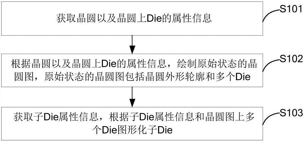
[0034] The embodiment of the present invention discloses a single-target and multi-target wafer map construction method, such as figure 1 shown, including the following steps:

[0035] Step S101, obtaining the attribute information of the wafer and Die on the wafer;

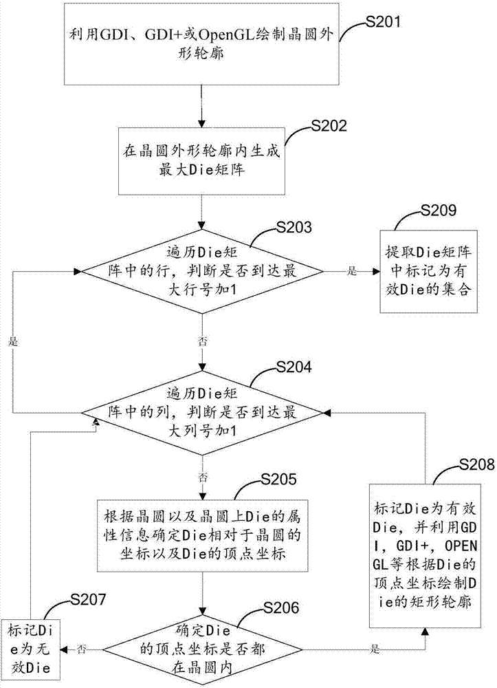
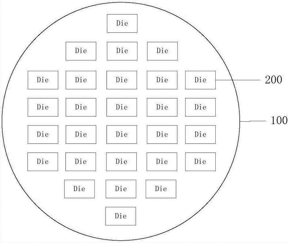
[0036] In the embodiment of the present invention, specifically, the wafer attribute information includes wafer diameter (Diameter, mm), height (Y, um) and width (X, um) of Die on the wafer, height deviation of Die on the wafer Offset (OffsetY, %) and width offset (OffsetX, %), routi...


PUM


Abstract

The invention provides a construction method for a single-project and multiple-project compatible wafer diagram. The construction method comprises the following steps of acquiring a wafer and attribute information of Die of the wafer, drawing a wafer diagram at an initial state according to the wafer and the attribute information of the Die of the wafer, the wafer at the initial state having a wafer profile and a plurality of dies, acquiring sub-Die attribute information, and drawing the sub-dies according to the sub-Die attribute information and the plurality of die diagrams on the wafer. With addition of die and sub-die type dimensions to a semiconductor wafer diagram, a problem that test of a whole multi-project wafer cannot be completed by a single test can be solved; test on the wholemulti-project wafer can be scanned for once by an external program according to retrieval of type information of the dies and the sub-dies without requirement of multi-stage. With a sub-die integrated layout drawing method in the die, the sub-die can be vividly displayed; and the construction method is easy to use.

Description

technical field [0001] The invention relates to the technical field of wafer map construction methods, in particular to a construction method with single-target and multi-target wafer map. Background technique [0002] In the semiconductor wafer test and measurement process, in order to achieve automated test and measurement, people often use a computer wafer (Wafer) diagram program to record and display the actual semiconductor wafer physical properties, measurement process and measurement results. Generally, the devices (Die) are arranged on the semiconductor according to a certain layout method, and the position, size and dimension of each device, and the direct spacing of the Die are all determined. Specifically, the wafer map mainly plays the following roles in the semiconductor wafer testing process: to describe the shape and physical dimensions of the semiconductor wafer (Wafer) map (diameter, gap or trim size, orientation, etc.); The physical size (length, width, et...

Claims


Application Information

Patent Timeline
Patent Type & Authority Applications(China)
IPC IPC(8): G06F17/50G06T11/20H01L21/66
Inventor 沈景山张海洋吕文波
Owner 苏州伊欧陆系统集成有限公司
Why Eureka
Try Eureka