A polarized waveguide transmission coupling device and preparation method based on in-plane heterojunction

A coupling device and heterojunction technology, applied in the direction of optical waveguide light guide, light guide, instrument, etc.

Active Publication Date: 2020-09-25
THE NAT CENT FOR NANOSCI & TECH NCNST OF CHINA
View PDF5 Cites 0 Cited by
  • Summary
  • Abstract
  • Description
  • Claims
  • Application Information

AI Technical Summary

Problems solved by technology

However, waveguide mode analysis and the conduction of polarized waves at the atomic scale of several layers or even a single layer have always been extremely challenging.

Method used


Image

  • A polarized waveguide transmission coupling device and preparation method based on in-plane heterojunction
  • A polarized waveguide transmission coupling device and preparation method based on in-plane heterojunction
  • A polarized waveguide transmission coupling device and preparation method based on in-plane heterojunction

Examples


Embodiment Construction

[0031] The objects and functions of the present invention and methods for achieving the objects and functions will be clarified by referring to the exemplary embodiments. However, the present invention is not limited to the exemplary embodiments disclosed below; it can be implemented in various forms. The essence of the description is only to help those skilled in the relevant art comprehensively understand the specific details of the present invention.

[0032] Hereinafter, embodiments of the present invention will be described with reference to the accompanying drawings. In the drawings, the same reference numerals represent the same or similar components, or the same or similar steps.

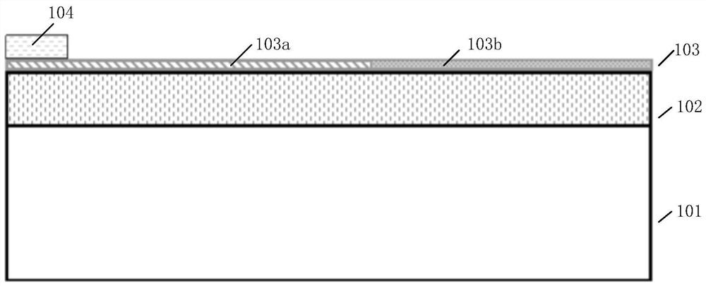
[0033] figure 1 Shown is the longitudinal section front view of the polarized waveguide transmission coupling device based on the in-plane heterojunction of the present invention.

[0034] Such as figure 1 As shown, the polarized waveguide transmission coupling device based on in-plane h...


PUM


Abstract

The invention discloses a polarized waveguide transmission coupling device based on an in-plane heterojunction. The transmission coupling efficiency is controllable. The device comprises a substrate,a dielectric layer, and a graphene / hBN in-plane heterojunction film, wherein the substrate, the dielectric layer and the graphene / hBN in-plane heterojunction film are successively arranged from bottomto top. The polarized waveguide transmission coupling device can change a momentum matching condition between a graphene Plasmon polarized wave and a hBN phonon polarized wave, thereby regulating thetransmission coupling efficiency between the polarized waves. When a graphene regulating femtometer reaches a momentum matching point of two polarized waves, the coupling efficiency between the polarized waves can reach 100%, thereby realizing 100% transmission.

Description

technical field [0001] The invention relates to the technical field of photonic integrated circuits, in particular to a device and method for transmission and coupling of plasmon polarized waves and phonon polarized wave guides on graphene / hBN in-plane heterojunctions. Background technique [0002] The photonic integrated circuit can overcome the optical diffraction limit, greatly reduce the scale of the device, and realize integration on the nanometer scale. At the same time, it uses optical signals to transmit information, which greatly reduces the loss in the transmission process. It has shown great potential and advantages, and it may be an important pillar of the new generation of information technology that replaces "integrated circuits". [0003] Graphene is a two-dimensional crystal composed of a single layer of carbon atoms, and graphite with less than ten layers is regarded as graphene. It has excellent electrical and optical properties, and has great application ...

Claims


Application Information

Patent Timeline
Patent Type & Authority Patents(China)
IPC IPC(8): G02B6/122G02B6/13
CPCG02B6/1226G02B6/13G02B2006/12061G02B2006/12147
Inventor 戴庆郭相东杨晓霞胡海胡德波廖宝鑫
Owner THE NAT CENT FOR NANOSCI & TECH NCNST OF CHINA
Why Eureka
Try Eureka