Multifunctional optoelectronic device

An optoelectronic device and multi-functional technology, applied in the field of electronics, can solve the problems of low integration and increase application cost, and achieve the effects of high response speed, low operating voltage and high energy efficiency

Active Publication Date: 2019-04-16
SHENZHEN UNIV
View PDF6 Cites 7 Cited by
  • Summary
  • Abstract
  • Description
  • Claims
  • Application Information

AI Technical Summary

Problems solved by technology

[0003] In order to solve the above-mentioned problems in the prior art, the present invention provides a multi-functional optoelectronic device to solve the problem that the existing optoelectronic device does not realize the integration of multiple functions into a single device structure, the degree of integration is low, and the application Cost and other issues

Method used


Image

  • Multifunctional optoelectronic device
  • Multifunctional optoelectronic device
  • Multifunctional optoelectronic device

Examples


Embodiment Construction

[0031] The present invention will be further described below in conjunction with the accompanying drawings and specific embodiments. Terms such as "upper", "lower", "left", "right", "middle" and "one" quoted in the preferred embodiment are only for convenience of description, and are not used to limit the scope of the present invention. The scope of implementation and the change or adjustment of its relative relationship shall also be regarded as the scope of implementation of the present invention without substantive changes in technical content.

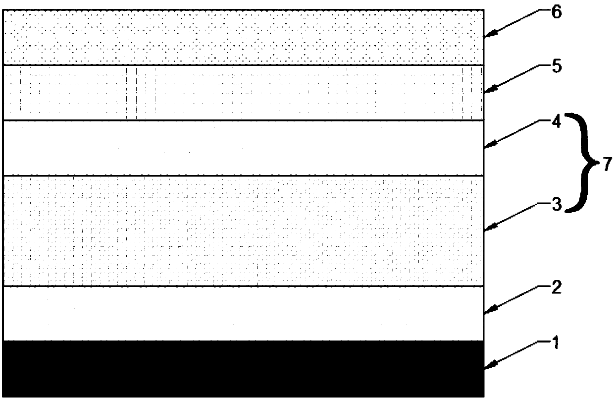
[0032] like figure 1 As shown, the multifunctional optoelectronic device includes ITO glass 1, hole transport layer 2, heterojunction 7, electron transport layer 5 and metal electrode 6, and the ITO glass 1 is the substrate of the entire optoelectronic device, and the ITO glass 1 A hole transport layer 2, a heterojunction 7, and an electron transport layer 5 are sequentially arranged on the top from bottom to top, or an electron t...


PUM


Abstract

A multifunctional optoelectronic device comprises ITO glass, a hole transport layer, a heterojunction, an electron transport layer and a metal electrode, wherein the ITO glass is a substrate of the entire optoelectronic device; the hole transport layer, the heterojunction, and the electron transport layer are successively disposed on the ITO glass from bottom to top, or the electron transport layer, the heterojunction, and the hole transport layer are successively disposed on the ITO glass from bottom to top; the surface of the electron transport layer or the hole transport layer at the uppermost layer is plated with the metal electrode; the heterojunction is formed by stacking a perovskite layer and a quantum dot layer; the hole transport layer forms a P-type semiconductor; the heterojunction forms an intrinsic semiconductor; and the electron transport layer forms an N-type semiconductor such that the optoelectronic device has a PIN structure and a built-in electric field from the electron transport layer to the hole transport layer is generated in the optoelectronic device. The multifunctional optoelectronic device of the invention can realize energy collection, energy injectionand energy detection functions on a single device structure.

Description

technical field [0001] The invention relates to the field of electronic technology, in particular to a multifunctional optoelectronic device for mutual conversion between light energy and electric energy. Background technique [0002] As the application fields of optoelectronic devices become wider and wider, the demand for light weight, integration and multi-functionalization of optoelectronic devices in this era is also increasing. For example, it is becoming more and more important to integrate multiple optoelectronic devices into one system more important. In the prior art, optoelectronic devices have not yet efficiently integrated the advantages of low energy consumption, low operating voltage, high response speed, high energy efficiency, high-quality continuous light, and energy collection, injection, and detection into a single device structure, and Electronic devices in the prior art not only have a large area, but also various functions need to be realized by diffe...

Claims


Application Information

Patent Timeline
Patent Type & Authority Applications(China)
IPC IPC(8): H01L51/42H01L51/50
CPCH10K30/152H10K50/115Y02E10/549
Inventor 李贵君任鐾韬阮锦昌江乐周定坚徐浩
Owner SHENZHEN UNIV
Why Eureka
Try Eureka