A kind of ped sample and preparation method thereof

A sample and sample preparation technology, which is applied in the direction of instruments, measuring devices, scientific instruments, etc., can solve the problem of low measurement accuracy of polysilicon layer grain size, and achieve the effect of improving measurement accuracy

Active Publication Date: 2022-07-22
YANGTZE MEMORY TECH CO LTD
View PDF0 Cites 0 Cited by
  • Summary
  • Abstract
  • Description
  • Claims
  • Application Information

AI Technical Summary

Problems solved by technology

However, the measurement accuracy of the polysilicon layer grain size measured by this PED sample is not high

Method used


Image

  • A kind of ped sample and preparation method thereof
  • A kind of ped sample and preparation method thereof
  • A kind of ped sample and preparation method thereof

Examples


preparation example Construction

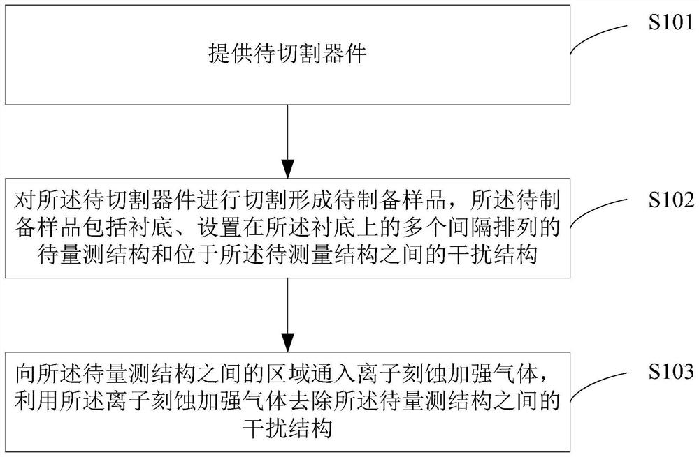
[0031] Based on this, the present invention provides a method for preparing a PED sample to overcome the above-mentioned problems existing in the prior art, including:

[0032] Provide devices to be cut;

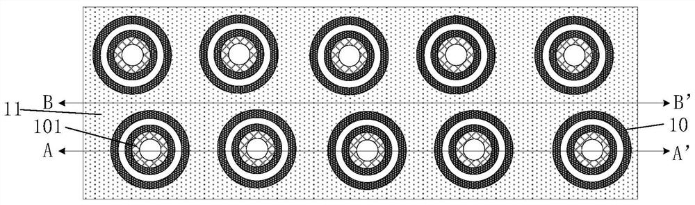
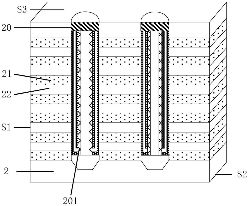
[0033] Cutting the to-be-cut device to form a to-be-prepared sample, the to-be-prepared sample includes a substrate, a plurality of spaced apart structures to be measured disposed on the substrate, and interference between the structures to be measured structure;

[0034] An ion-etching enhancement gas is introduced into the region between the structures to be measured, and the ion-etching enhancement gas is used to remove interference structures between the structures to be measured.

[0035] In the preparation method of the PED sample provided by the present invention, an ion-etching enhanced gas is introduced into the area between the structures to be measured, and the ion-etched enhanced gas is used to remove the interfering structures between the structures to be measu...


PUM


Abstract

The present invention provides a PED sample and a preparation method thereof, including: providing a device to be cut; cutting the device to be cut to form a sample to be prepared, and the sample to be prepared includes a substrate and a A plurality of spaced apart structures to be measured and interfering structures located between the structures to be measured; passing ion-etching enhanced gas into the region between the to-be-measured structures, and using the ion-etched enhanced gas to remove The interference structure between the structures to be measured can eliminate the influence of the interference structure on the measurement accuracy of the structure to be measured, thereby improving the measurement accuracy of the grain size of the structure to be measured, such as the polysilicon layer in the channel hole .

Description

technical field [0001] The present invention relates to the technical field of semiconductor manufacturing, and more particularly, to a PED sample and a preparation method thereof. Background technique [0002] In the manufacturing process of three-dimensional memory (3D NAND), in order to use Transmission Electron Microscope (TEM) to measure the grain size of the polysilicon layer in the channel hole, it is necessary to prepare a special PED (Precession Electron Diffraction, precession) for TEM. electron diffraction) samples. [0003] In order to measure the grain size of the polysilicon layer in the channel hole of the PED sample, it is generally used such as figure 1 The cutting method shown is that half of the channel hole 10 is cut along the cutting lines AA' and BB', so that a larger area can be obtained, and the overlapping of the polysilicon layers 101 of the front and rear layers can be avoided. However, the measurement accuracy of the grain size of the polysilico...

Claims


Application Information

Patent Timeline
Patent Type & Authority Patents(China)
IPC IPC(8): G01N23/20058G01N23/20008
CPCG01N23/20058G01N23/2005
Inventor 邹锭
Owner YANGTZE MEMORY TECH CO LTD
Why Eureka
Try Eureka