Full-electronic-control two-dimensional light beam scanning device

A technology of beam scanning and scanning devices, which is applied in the field of optical phased arrays, can solve problems such as high power consumption and complex control, and achieve the effects of alleviating heat dissipation pressure, reducing chip power consumption, and saving laser costs

Active Publication Date: 2020-07-10
HUAZHONG UNIV OF SCI & TECH
View PDF5 Cites 6 Cited by
  • Summary
  • Abstract
  • Description
  • Claims
  • Application Information

AI Technical Summary

Problems solved by technology

[0007] The purpose of the present invention is to provide a fully electronically controlled two-dimensional beam scanning device, which solves the problems of complex control and high power consumption in traditional two-dimensional optical phased array systems through hybrid integration

Method used


Image

  • Full-electronic-control two-dimensional light beam scanning device
  • Full-electronic-control two-dimensional light beam scanning device
  • Full-electronic-control two-dimensional light beam scanning device

Examples


Embodiment Construction

[0023] In order to make the object, technical solution and advantages of the present invention clearer, the specific implementation manners of the present invention will be further described in detail below in conjunction with examples. It should be understood that the embodiments described here are only used to explain the present invention, but not to limit the scope of the present invention.

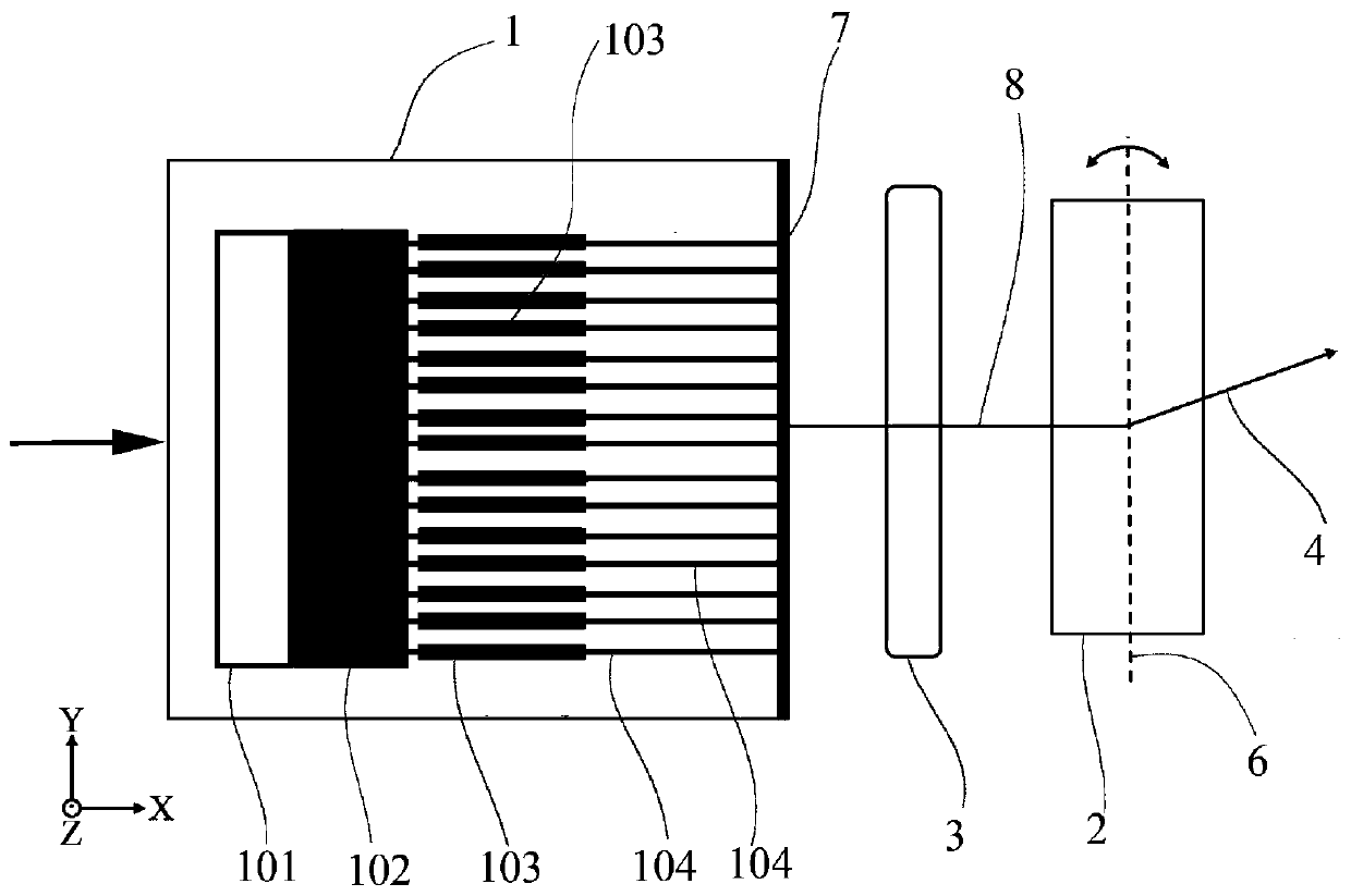
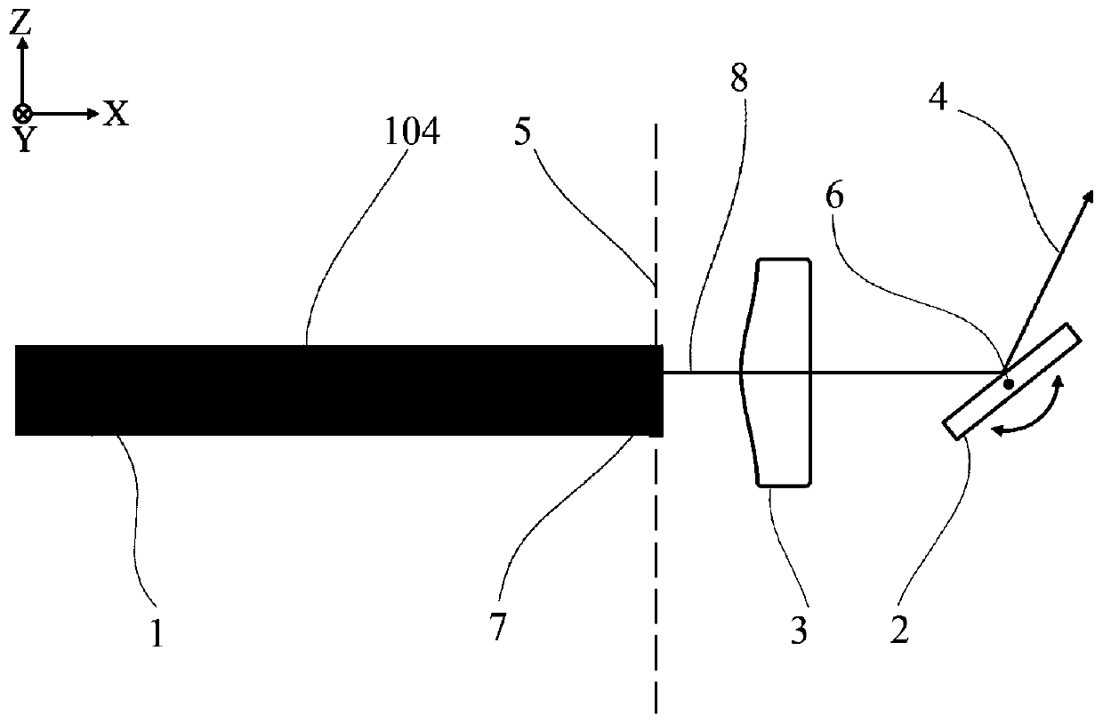
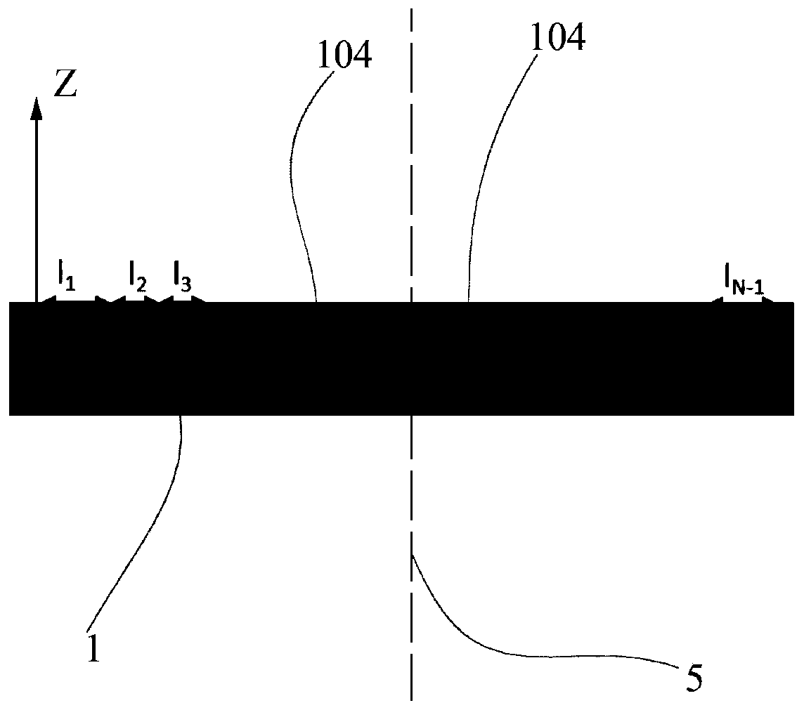
[0024] A fully electronically controlled two-dimensional beam scanning device in one embodiment of the present invention includes a laser, a one-dimensional waveguide phased array 1, a MEMS mirror 2 and a control chip, wherein the laser is used to emit a laser beam. figure 1 with figure 2 It is a schematic structural diagram of a fully electronically controlled two-dimensional beam scanning device in the X-Y direction and X-Z direction according to an embodiment of the present invention. It can be seen from the figure that the one-dimensional waveguide phased array 1 is used to gene...


PUM


Abstract

The invention provides a full-electronic-control two-dimensional light beam scanning device. The device comprises a laser, a one-dimensional waveguide phased array, a cylindrical lens, an MEMS reflector and a control chip. The one-dimensional waveguide phased array is used for generating a one-dimensional first scanning light beam from an incident laser beam through the phased array. The first scanning light beam is shaped by the cylindrical lens and then reflected to a free space by the MEMS reflector, the MEMS reflector rotates around an axis, and the one-dimensional waveguide phased array and the MEMS reflector are electrically connected to a control chip to control a second scanning light beam emitted from the MEMS reflector to realize full-space two-dimensional scanning. According tothe two-dimensional light beam scanning device provided by the invention, the one-dimensional phased array and the MEMS reflector are integrated in a mixed manner, and full-space two-dimensional scanning of laser beams is realized. Compared with a traditional two-dimensional phased array system, the device has the advantages that the laser cost is saved, the workload of a control chip is reduced,the power consumption of the chip is reduced, the heat dissipation pressure is relieved, and miniaturization and integration of the system are facilitated.

Description

technical field [0001] The invention belongs to the technical field of optical phased arrays, in particular to a hybrid integrated two-dimensional light beam deflection device. Background technique [0002] Similar to traditional microwave radar using microwave scanning, lidar searches and tracks targets by controlling the deflection of laser beams, and then achieves the purpose of obtaining information such as target distance, azimuth and speed. However, due to its high resolution in the time domain, frequency domain and air domain, coupled with its good concealment and small size, it has rapidly gained wide application and attention in the field of target detection. However, the current traditional mechanical scanning lidar is increasingly unable to meet the requirements of high-performance radar due to its relatively complex system and low mechanical scanning speed caused by inertia. [0003] People began to study microwave phased array technology very early, and the con...

Claims


Application Information

Patent Timeline
Patent Type & Authority Applications(China)
IPC IPC(8): G01S17/66G01S7/481
CPCG01S7/4817G01S17/66
Inventor 国伟华谈苏陆巧银
Owner HUAZHONG UNIV OF SCI & TECH
Why Eureka
Try Eureka