An ultraviolet wide-spectrum lithography lens

A wide-spectrum, ultraviolet light source technology, applied in the field of circuit board lithography, can solve the problem of high cost of use, achieve good stability, easy debugging of the whole machine, and satisfactory imaging quality

Active Publication Date: 2021-03-23
安徽国芯智能装备有限公司
View PDF5 Cites 0 Cited by
  • Summary
  • Abstract
  • Description
  • Claims
  • Application Information

AI Technical Summary

Problems solved by technology

[0004] However, the working wavelength of the laser used in the existing PCB lithography technology is generally 405nm, which requires a special dry film, and the lens used is also a single-wavelength lens, which cannot solve the problem of high cost of the existing technology.

Method used


Image

  • An ultraviolet wide-spectrum lithography lens
  • An ultraviolet wide-spectrum lithography lens
  • An ultraviolet wide-spectrum lithography lens

Examples


Embodiment 1

[0126] Table 1 is a summary table of optical parameters of each lens in the lithography lens provided by the embodiment of the present invention, as shown in Table 1,

[0127] Table 1

[0128]

[0129]

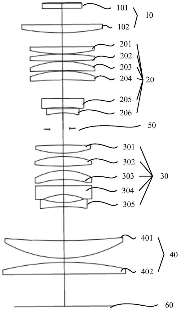
[0130] It should be noted that the serial number of each surface is figure 1 The sequence number of each side surface distributed according to the order from the object side of the digital micromirror 101 to the object side of the fourteenth lens 402: for example, S1 is the object side sequence number of the digital micromirror 101; S2 is the number of the first lens 102 The serial number of the object side; S3 is the serial number of the image side of the first lens 102; S4 is the serial number of the object side of the second lens 201; S5 is the serial number of the image side of the second lens 201.

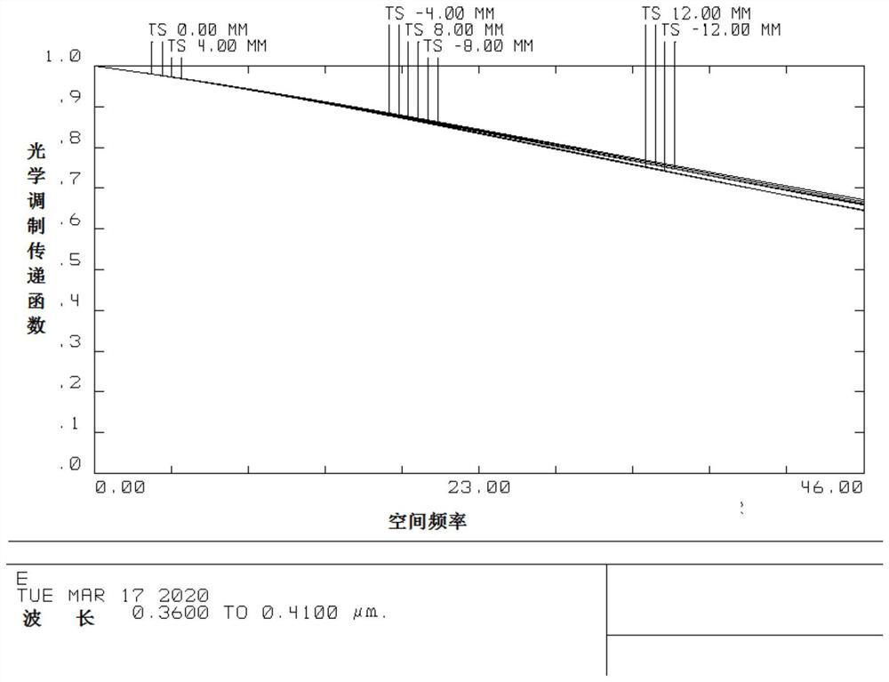
[0131] figure 2 The MTF (ModulationTransfer Function, modulation transfer function) figure of a kind of ultraviolet wide-spectrum lithography lens that the embodiment...


PUM

PropertyMeasurementUnit
wavelengthaaaaaaaaaa

Abstract

An ultraviolet wide-spectrum photoetching lens is characterized in that the lens comprises an ultraviolet light source, a first lens group, a second lens group, a third lens group and a fourth lens group which are sequentially arranged from the ultraviolet light source to a target, the ultraviolet light source comprises a digital micro-reflector and a first lens, and the first lens is a biconvex lens; the first lens group comprises a first number of positive lenses and a second number of negative lenses which are sequentially arranged from the ultraviolet light source to the target, and the combined focal length of the first lens group is positive; the second lens group comprises a third number of positive lenses and a fourth number of negative lenses which are sequentially arranged from the ultraviolet light source to the target, the combined focal length of the second lens group is positive, and the lens, closest to the first lens group, in the second lens group can move in the direction of the optical axis; the third lens group comprises a fifth number of positive lenses which are sequentially arranged from the ultraviolet light source to the target, and the combined focal length of the third lens group is positive. By applying the embodiment of the invention, the photoetching cost can be reduced.

Description

technical field [0001] The invention relates to the technical field of circuit board lithography, in particular to an ultraviolet wide-spectrum lithography lens. Background technique [0002] At present, as the demand for high-density circuit boards continues to increase, the traditional PCB (Printed Circuit Board, printed circuit board) contact exposure machine can no longer meet the high-density demand, and the mask needs to be replaced frequently, resulting in high cost of use. Therefore, a new digital exposure machine is commonly used at present, but this digital exposure machine usually uses a single-wavelength ultraviolet laser light source. A special dry film is required, and the price of a special dry film is much higher than that of an ordinary dry film. Therefore, the existing digital lithography machine has a technical problem of high lithography cost. [0003] In order to solve the above problems, the invention patent application with the application number of 2...

Claims


Application Information

Patent Timeline
Patent Type & Authority Patents(China)
IPC IPC(8): G03F7/20
CPCG03F7/2004G03F7/70241G03F7/70258
Inventor 李文静薛业保章广飞王运钢
Owner 安徽国芯智能装备有限公司
Why Eureka
Try Eureka