Ultra-wide-spectrum wave-absorbing material and preparation method thereof

An absorbing material and ultra-broad spectrum technology, applied in the field of absorbing materials, can solve the problems of difficult broadband absorbing effect, unable to form multiple absorbing coupling peaks, small absorbing frequency bandwidth, etc. The effect of reducing dependence and widening the absorption bandwidth

Active Publication Date: 2020-12-01
SHENZHEN JIACHEN TECH
View PDF13 Cites 4 Cited by
  • Summary
  • Abstract
  • Description
  • Claims
  • Application Information

AI Technical Summary

Problems solved by technology

[0005] The embodiment of the present invention aims at the fact that the above-mentioned existing multi-layer absorbing material cannot form multiple absorbing coupling peaks, the absorbing frequency bandwidth is small, and it is difficult to achieve broadband Problems with absorbing effect, providing an ultra-broadband absorbing material and its preparation method

Method used


Image

  • Ultra-wide-spectrum wave-absorbing material and preparation method thereof
  • Ultra-wide-spectrum wave-absorbing material and preparation method thereof
  • Ultra-wide-spectrum wave-absorbing material and preparation method thereof

Examples


Embodiment Construction

[0030] In order to make the object, technical solution and advantages of the present invention clearer, the present invention will be further described in detail below in conjunction with the accompanying drawings and embodiments. It should be understood that the specific embodiments described here are only used to explain the present invention, not to limit the present invention.

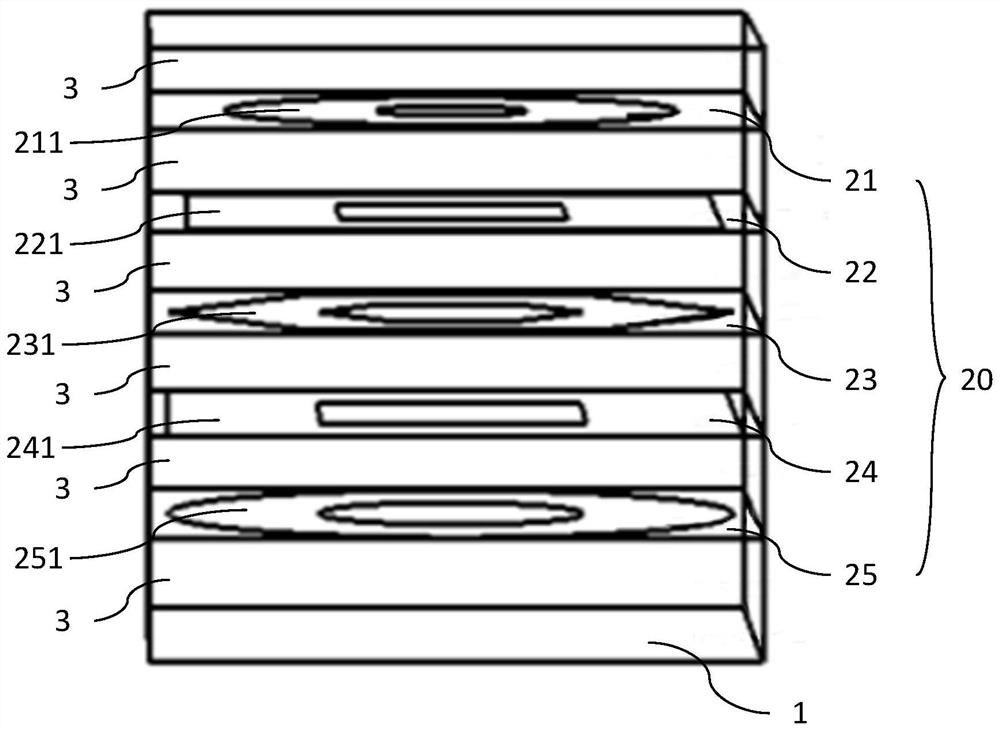
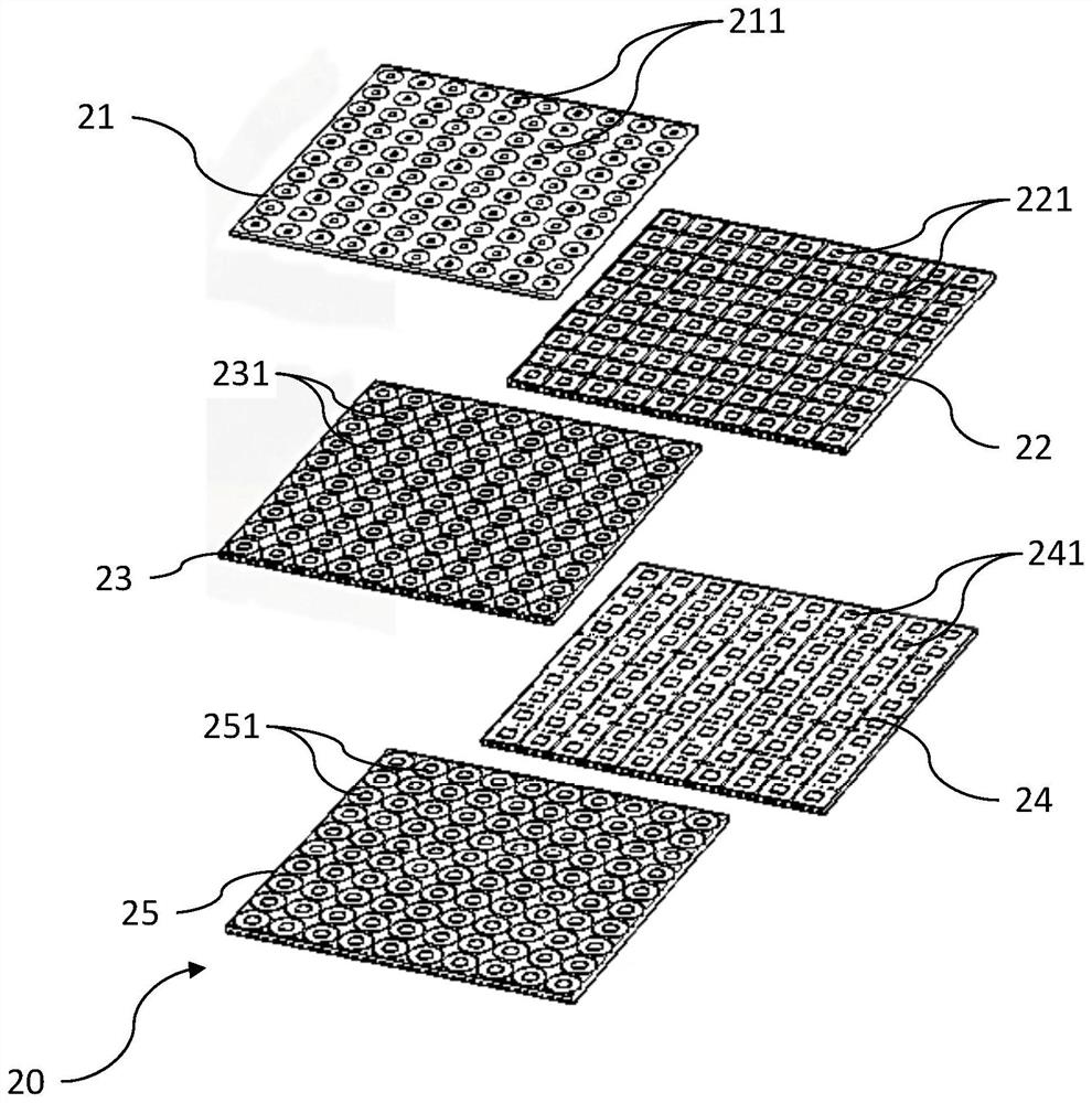
[0031] like figure 1 Shown is a schematic diagram of the partial structure of the ultra-broadband absorbing material provided by the embodiment of the present invention, which can be applied to the field of absorbing materials, especially in microwave anechoic chambers and radio anechoic chambers used for research and development, and It is used in electromagnetic shielding boxes or small and medium-sized shielded darkrooms for production line testing. The ultra-broad-spectrum absorbing material in this embodiment includes a metal backplane 1, a plurality of absorbing structure layers 20 and a plu...


PUM

PropertyMeasurementUnit
thicknessaaaaaaaaaa
thicknessaaaaaaaaaa
thicknessaaaaaaaaaa

Abstract

The invention provides an ultra-wide-spectrum wave-absorbing material and a preparation method thereof. The ultra-wide-spectrum wave-absorbing material comprises a metal backboard, a plurality of wave-absorbing structure layers and a plurality of dielectric layers, wherein a dielectric layer is arranged between two adjacent wave-absorbing structure layers; each wave-absorbing structure layer comprises a plurality of wave-absorbing units, each wave-absorbing unit comprises a resistive film structure, and the vertical projections of the wave-absorbing units of the plurality of wave-absorbing structure layers are the same; the resistive film structures of the multiple wave-absorbing structure layers are arranged in a preset annular geometrical shape, the sizes and / or geometrical shapes of theresistive film structures of every two adjacent wave-absorbing structure layers are different, and electromagnetic waves with different frequency spectrums are absorbed through the resistive film structures with different sizes and / or geometrical shapes. By forming a plurality of wave-absorbing coupling peaks, the absorbing capacity of the wave-absorbing material to electromagnetic waves is enhanced, the wave-absorbing frequency band width is widened, the broadband wave-absorbing effect can be achieved, and the dependence of the wave-absorbing material on the oblique incident angle of the electromagnetic waves is reduced.

Description

technical field [0001] The embodiments of the present invention relate to the field of wave-absorbing materials, and more specifically, to an ultra-broad-spectrum wave-absorbing material and a preparation method thereof. Background technique [0002] With the vigorous development of the electronics industry and the upgrading of 5G communication technology, various basic equipment related to 5G communication (such as base stations, antenna arrays, etc.), as well as various smart homes, mobile phones, bracelets, Bluetooth headsets and automatic driving The research and development and production testing of products, etc., all need to be carried out in a specific clean electromagnetic environment. There are usually microwave anechoic chambers and radio anechoic chambers for research and development, as well as electromagnetic shielding boxes or small and medium-sized shielded anechoic chambers for production line testing, and the core of all these test application scenarios is ...

Claims


Application Information

Patent Timeline
Patent Type & Authority Applications(China)
IPC IPC(8): H05K9/00
CPCH05K9/0088
Inventor 李虎权聂晶周福兰伍连保
Owner SHENZHEN JIACHEN TECH
Why Eureka
Try Eureka