

Display device
a display device and liquid crystal technology, applied in the field of display devices, can solve the problems of complicated shape of the display device casing, and achieve the effect of reducing the frame width
- Summary
- Abstract
- Description
- Claims
- Application Information
AI Technical Summary
Benefits of technology
Problems solved by technology
Method used
Image

Examples
first embodiment
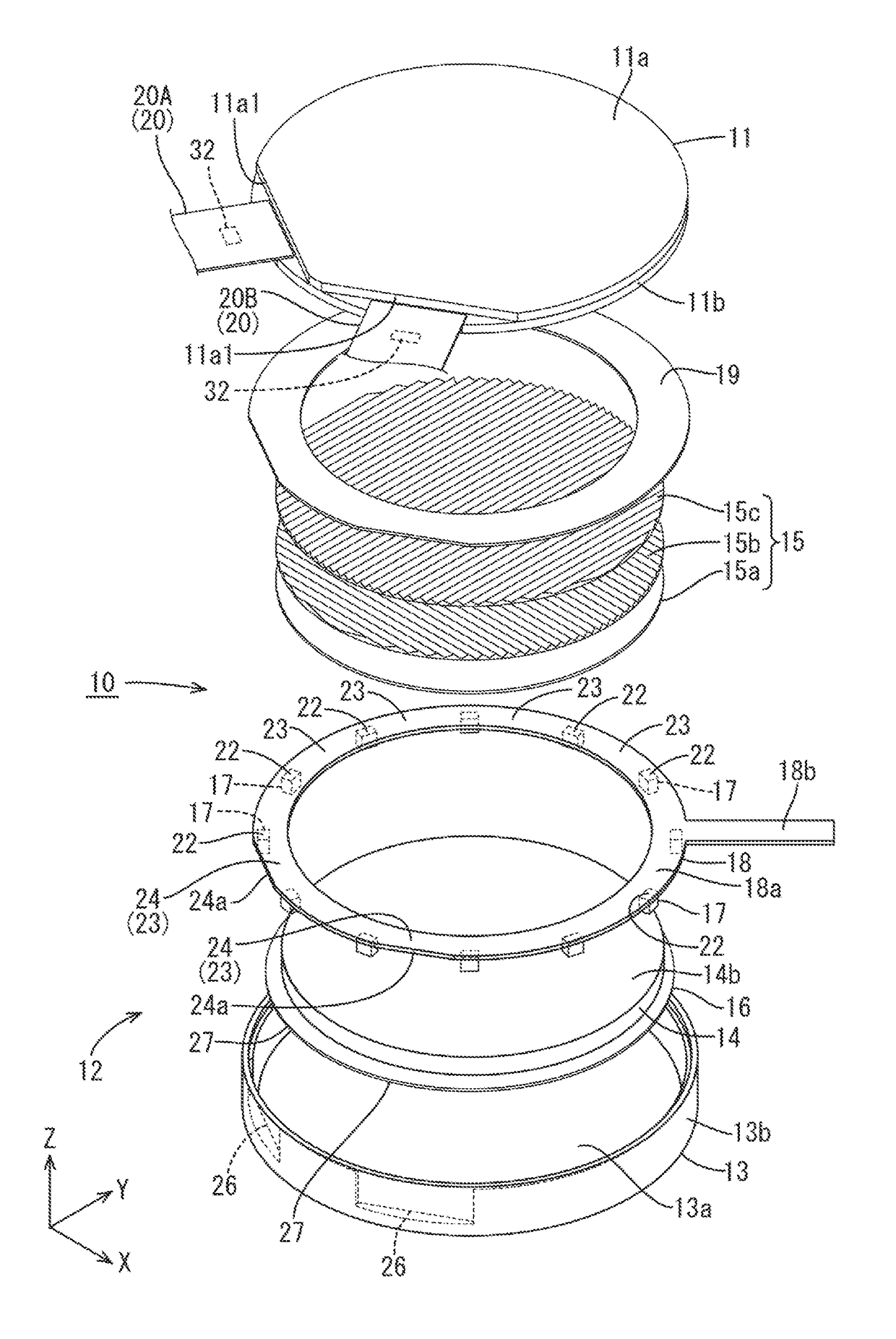
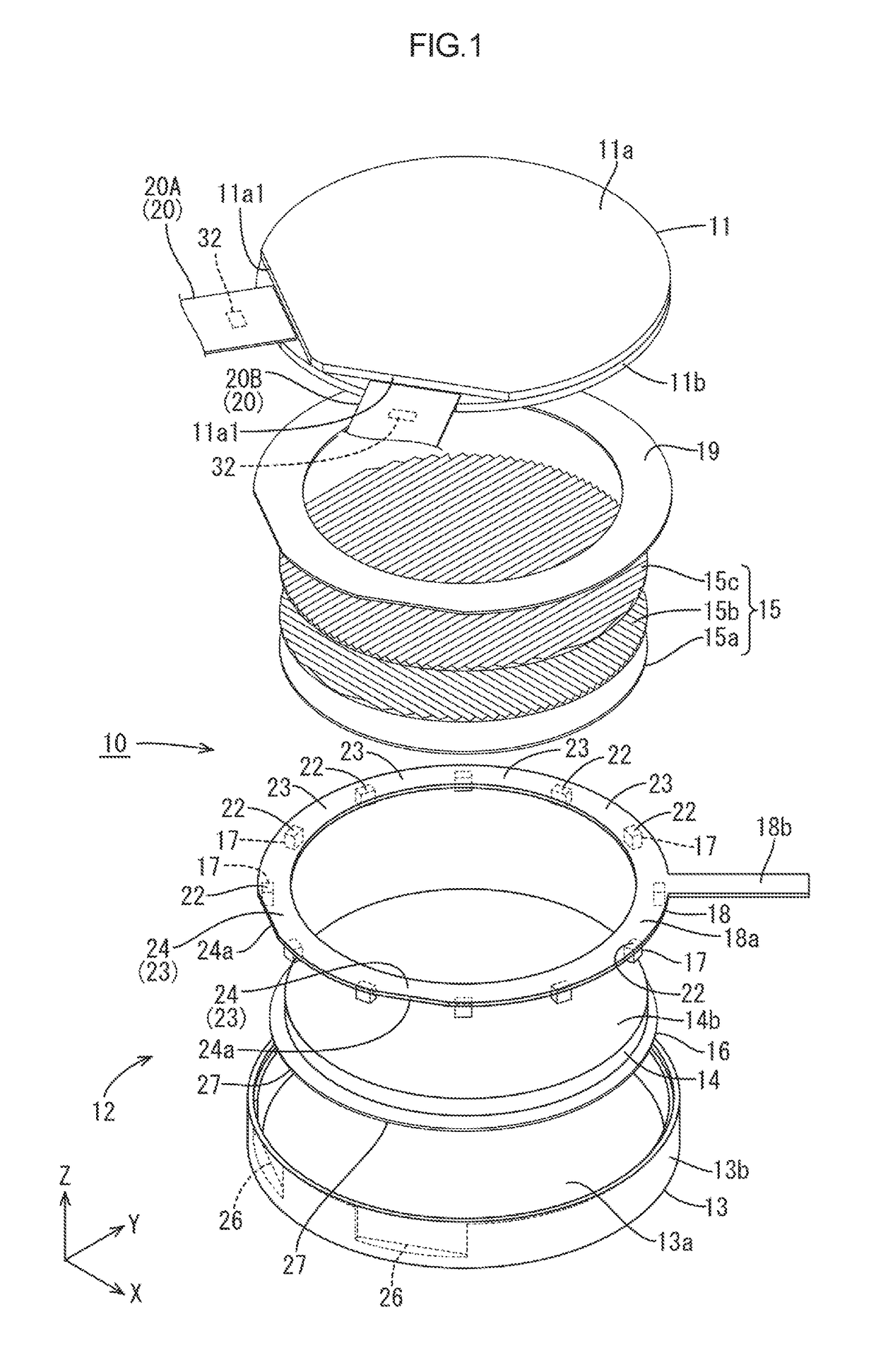
[0053]A first embodiment will be described with reference to FIGS. 1 to 11. In the present embodiment, a liquid crystal display device (a display device) 10 including a liquid crystal panel 11 as a display panel will be described. X-axis, Y-axis and Z-axis may be indicated in the drawings. The axes in each drawing correspond to the respective axes in other drawings. A vertical direction in FIGS. 8 and 9 is a reference vertical direction and an upper side and a lower side in FIGS. 8 and 9 are a front side and a rear side, respectively.
[0054]As illustrated in FIG. 1, the liquid crystal display device 10 has a substantially circular shape as a whole. The liquid crystal display device 10 at least includes a liquid crystal panel (a display panel) 11 for displaying images thereon, and a backlight device (a lighting device) 12 arranged on a rear side with respect to the liquid crystal panel 11 and providing light toward the liquid crystal panel 11. The liquid crystal display device 10 may ...
second embodiment
[0091]A second embodiment of the present invention will be described with reference to FIG. 12 or 13. In the second embodiment, arrangement of the gate circuit portion GDM is altered. Configurations, operations, and effects similar to those of the first embodiment will not be described.
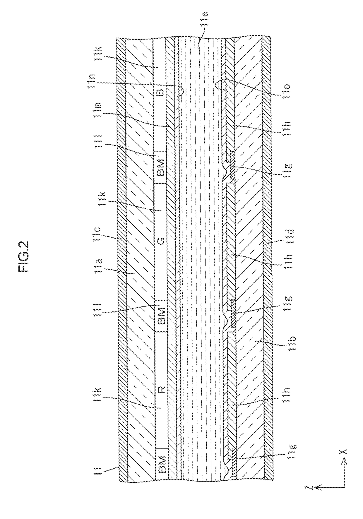
[0092]As illustrated in FIGS. 12 and 13, the gate circuit portion GDM of the present embodiment is arranged in the non-display area NAA of an array substrate 111b of a liquid crystal panel 111. The gate circuit portion GDM includes a control circuit (such as circuit TFTs and circuit lines) and at least a part of the control circuit has light-blocking properties. All the gate circuit portion GDM including a light-blocking portion are arranged in the non-display area NAA and the transmission rate of light and the aperture ratio of each pixel in the display area are increased. The gate circuit portion GDM extends along the outline of the display area AA in the non-display area NAA and has a substantially...
third embodiment
[0094]A third embodiment of the present invention will be described with reference to FIG. 14 or 15. In the third embodiment, arrangement of drivers 232 differs from that of the first embodiment. Configurations, operations, and effects similar to those of the first embodiment will not be described.
[0095]As illustrated in FIGS. 14 and 15, drivers 232 of the present embodiment are arranged in the non-display area NAA of an array substrate 211b of a liquid crystal panel 211. Therefore, the drivers 232 are not mounted on flexible printed circuit boards 220. Each of the drivers 232 is directly mounted on a portion of the array substrate 21b in the non-display area NAA between panel-side terminals 228 and the display area AA with the COG (chip on glass) mounting technology. Driver terminals (not illustrated) that are connected to terminals on the drivers 232 and relay lines (not illustrated) that connect the driver terminals and the panel-side terminals 228 are mounted in driver 232 mount...
PUM
| Property | Measurement | Unit |
|---|---|---|
| central angle | aaaaa | aaaaa |
| central angle | aaaaa | aaaaa |
| height | aaaaa | aaaaa |
Abstract
Description
Claims
Application Information