
Substrate and display device

a display device and substrate technology, applied in the field of substrates and display devices, can solve the problems of affecting the narrow frame design of the display device, prior art possesses drawbacks, and is in urgent need of improvement, so as to reduce the frame width of the non-display area, improve user experience, and increase the screen occupation ratio of the display device

Active Publication Date: 2021-07-22
WUHAN CHINA STAR OPTOELECTRONICS SEMICON DISPLAY TECH CO LTD
View PDF2 Cites 1 Cited by
  • Summary
  • Abstract
  • Description
  • Claims
  • Application Information

AI Technical Summary

Benefits of technology

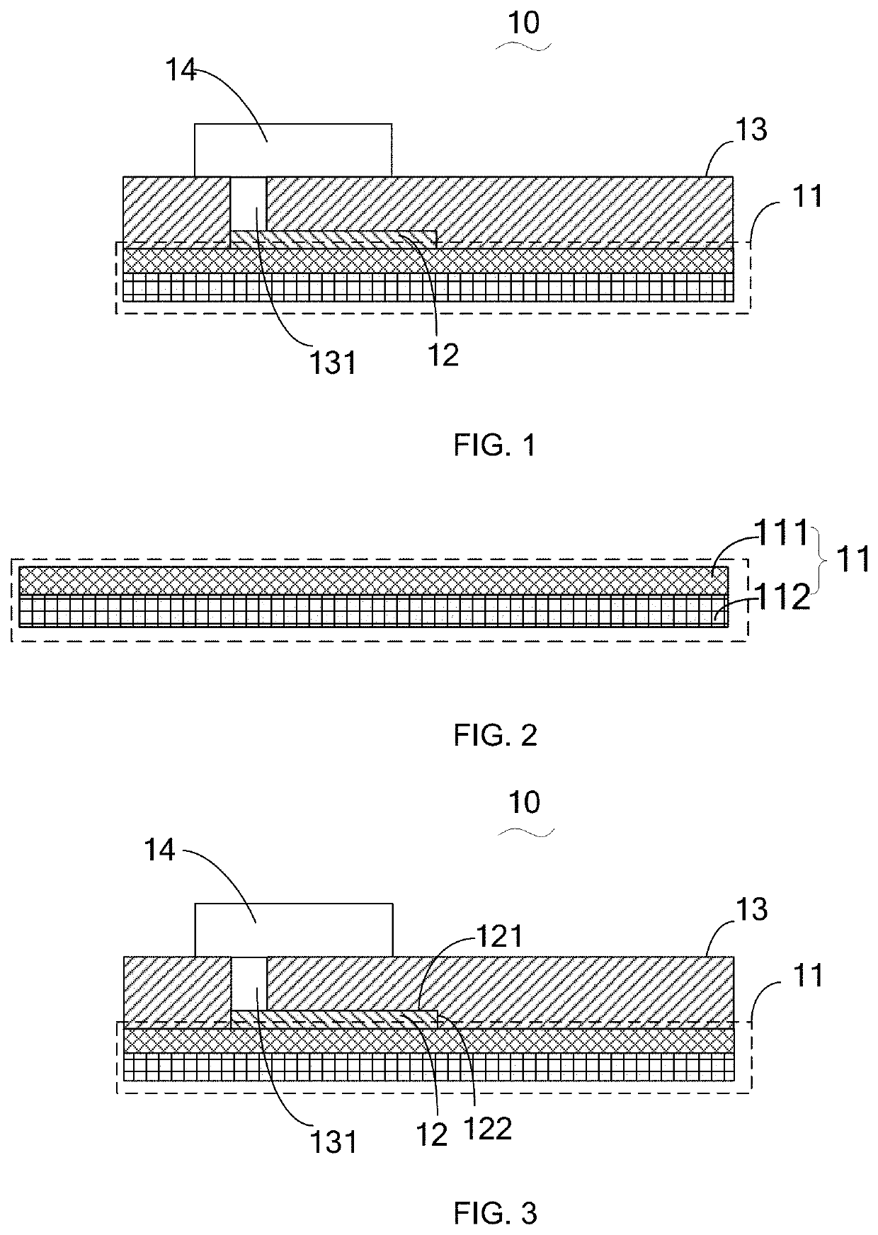
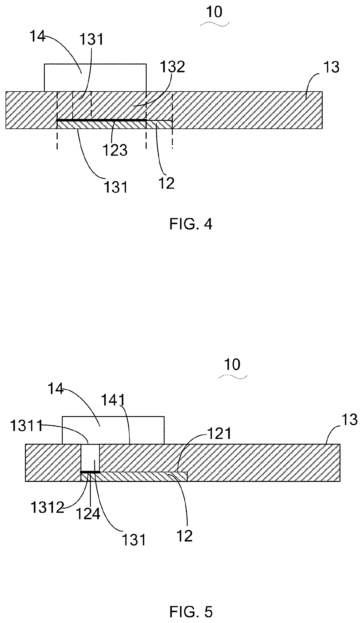
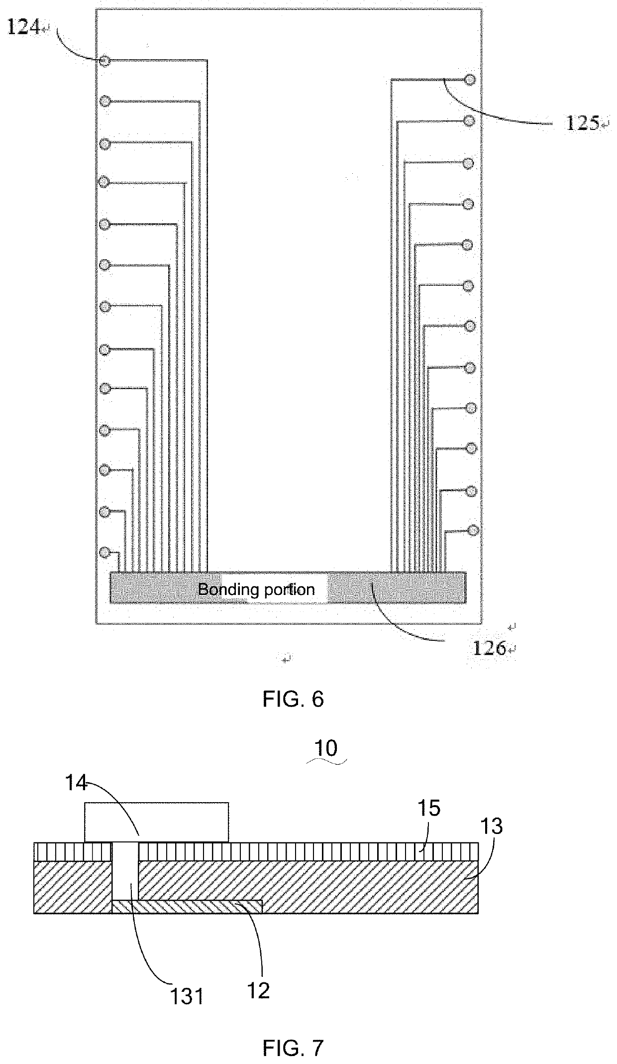
The present invention provides a substrate and display device that can achieve a narrow frame design by effectively reducing the width of traces on both sides of the display area. The substrate has a base substrate, wiring layer, flexible layer and gate driver on array circuit sequentially stacked from bottom to top. The wiring layer is in the substrate, and the peripheral wiring of the gate driver on array circuit is connected to the wiring layer with a through hole in the flexible layer. This reduces the frame width of the non-display area, increases the screen occupation ratio of the display device, and improves user experience.

Problems solved by technology

However, due to the use of GOA technology, the presence of GOA circuits and peripheral circuitry can affect the narrow frame design of the display device.
Therefore, the prior art possesses drawbacks and is in urgent need of improvement.

Method used


Image

  • Substrate and display device
  • Substrate and display device
  • Substrate and display device

Examples


Embodiment Construction

[0039]For better explaining the technical solution and the effect of the present invention, the present invention will be further described in detail with the accompanying drawings in the specific embodiments. It is clear that the described embodiments are merely part of embodiments of the present invention, but not all embodiments. Based on the embodiments of the present invention, all other embodiments to those of ordinary skill in the premise of no creative efforts obtained, should be considered within the scope of protection of the present invention.

[0040]In the description of the present invention, it is to be understood that the terms “center”, “longitudinal”, “transverse”, “length”, “width”, “thickness”, “upper”, “lower”, “front”, “Orientation of “post”, “left”, “right”, “vertical”, “horizontal”, “top”, “bottom”, “inside”, “outside”, “clockwise”, “counterclockwise”, etc. are positional relationships based on the orientations or positional relationships shown in the drawings, ...


PUM

PropertyMeasurementUnit
flexibleaaaaaaaaaa
widthaaaaaaaaaa
thicknessaaaaaaaaaa

Abstract

Disclosed are a substrate and a display device. The substrate includes: a base substrate, a wiring layer, a flexible layer and a gate driver on array circuit, which are sequentially stacked from bottom to top; wherein one side of the wiring layer is provided with a through hole penetrating the flexible layer to expose the gate driver on array circuit, so that the gate driver on array circuit is electrically connected to the wiring layer with the through hole.

Description

FIELD OF THE INVENTION[0001]The present invention relates to a display field, and more particularly to a substrate and a display device.BACKGROUND OF THE INVENTION[0002]In recent years, the organic light emitting diode (OLED) possesses many excellent characteristics, such as self-illumination, low energy consumption, wide viewing angle, rich color, fast response and flexible screen preparation, and thus causes great interest in the field of scientific research and industry, and is considered to be a promising next-generation display technology. With the advent of the big screen era, many display manufacturers are conducting narrow frame designs.[0003]In the prior art, the appearance of various technologies, such as a Gate Driver on Array (GOA) effectively reduces the frame width of the display device, thus greatly enriching the requirements of the narrow frame design. The flexible OLEDs are superior to liquid crystal displays (LCDs) in their narrow frame portions because of the flex...

Claims


Application Information

Patent Timeline
Patent Type & Authority Applications(United States)
IPC IPC(8): H01L27/32H01L51/00
CPCH01L27/3276H01L2251/5338H01L51/0097H01L27/124H10K59/122H10K59/131H10K77/111H10K2102/311G09G2300/0804G09G2300/0408G06F1/1652G09F9/301H10K2102/00
Inventor XU, BINXU, HONGYU
Owner WUHAN CHINA STAR OPTOELECTRONICS SEMICON DISPLAY TECH CO LTD
Learn More