Liquid crystal display panel and liquid crystal display device

a liquid crystal display panel and display panel technology, applied in non-linear optics, instruments, optics, etc., can solve the problems of difficult to realize frame-width reduction, and the luminance of the backlight needs to be increased, so as to reduce the size of parts, reduce the effect of transmittance reduction and high designability

Active Publication Date: 2019-01-22
TRIVALE TECH LLC
View PDF11 Cites 0 Cited by
  • Summary
  • Abstract
  • Description
  • Claims
  • Application Information

AI Technical Summary

Benefits of technology

[0010]An object is to provide a liquid crystal display panel that suppresses reduction in transmittance, reduces the size of a part of a frame unused for mounting, and has high designability, and a liquid crystal display device including such a liquid crystal display panel.
[0012]It is possible to provide a liquid crystal display device of an FFS mode capable of frame-width reduction without deteriorating display performance.

Problems solved by technology

The gate wire and the source wire intersect in the display region, and hence mounting portions for a gate IC and a source IC and the routing wires are formed on at least two sides of the display region, thereby being difficult to realize frame-width reduction.
Further, even when the gate IC and the source IC are formed on only one side, the routing wires need to be formed on another side except the one side, still being difficult to realize frame-width reduction (Japanese Patent Application Laid-Open No. 9-311341 (1997)).
Further, luminance of the backlight needs to be increased in order to compensate for reduction of luminance of a display device due to the reduction of transmittance, which may increase power consumption.
Particularly, in a case of the liquid crystal display device of an FFS mode, display is performed by applying a fringe electric field (oblique electric field containing both components of a horizontal electric field and a vertical electric field) to the liquid crystal layer, thus being liable to be affected by changes in electric field caused by wires in the periphery of the pixel electrode.

Method used


Image

  • Liquid crystal display panel and liquid crystal display device
  • Liquid crystal display panel and liquid crystal display device
  • Liquid crystal display panel and liquid crystal display device

Examples


Embodiment Construction

A. First Preferred Embodiment

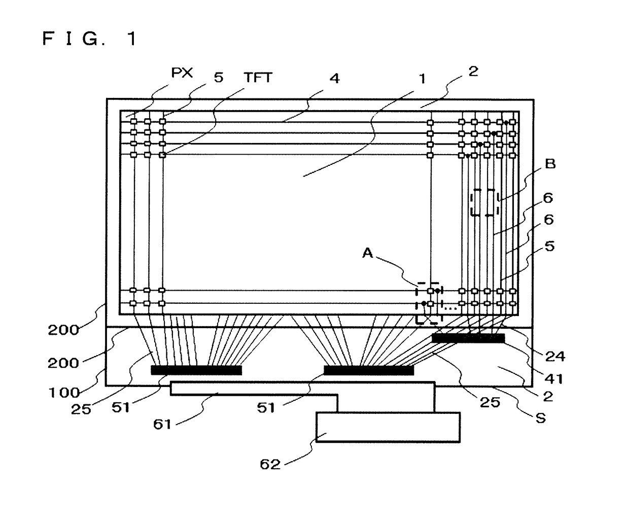
[0030]FIG. 1 is a plan view of a liquid crystal display panel according to a first preferred embodiment. As illustrated in FIG. 1, the liquid crystal display panel according to this first preferred embodiment includes a display region 1 corresponding to a display portion in which an image is displayed in a display device, and a frame region 2 being a periphery of the display region 1. In FIG. 1, a mode in which a TFT array substrate 100 and an opposing substrate 200 are overlapped is illustrated, and the opposing substrate 200 is overlapped at least with the display region 1. Although not shown, liquid crystals being an electro-optical material are sealed between both the substrates, which are sealed with a publicly-known method such as sealing so as not to allow the liquid crystals to be leaked. In the following description, components formed on the TFT array substrate 100 in FIG. 1 are mainly described.

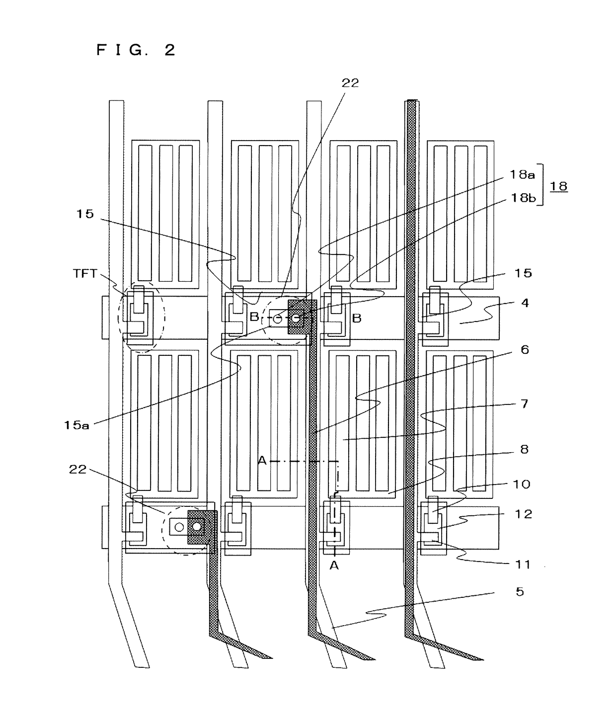
[0031]Horizontal wires extending in a horizontal d...


PUM

PropertyMeasurementUnit
thicknessaaaaaaaaaa
transparentaaaaaaaaaa
widthaaaaaaaaaa

Abstract

Gate connection lines connected to gate wires in a display region are formed so as to have a region overlapped with source wires. According to such a structure, both of frame-width reduction and display performance of a liquid crystal display panel may be realized.

Description

BACKGROUND OF THE INVENTIONField of the Invention[0001]The present invention relates to a liquid crystal display panel and a liquid crystal display device of a fringe field switching (FFS) mode.Description of the Background Art[0002]It has been a long time since new display devices have often been used, which include a display panel having a thin body and a planar shape through application of principals of liquid crystals, electroluminescence, and the like in place of a conventional cathode ray tube. A liquid crystal display device typifying such new display devices has characteristics in being capable of low voltage driving as well as having a thin body and light weight. The liquid crystal display device has a liquid crystal layer formed between two substrates. One of the substrates is an array substrate in which a plurality of pixels are arranged in a matrix pattern to form a display region. The other substrate is an opposing substrate in which color filters and the like are forme...

Claims


Application Information

Patent Timeline
Patent Type & Authority Patents(United States)
IPC IPC(8): G02F1/1333G02F1/1368G02F1/1343G02F1/1362
CPCG02F1/136286G02F1/1368G02F1/13439G02F1/134309G02F1/133345G02F2201/123G02F2001/134372G02F2201/121G02F1/1345G02F1/136227G02F1/134372
Inventor HASHIGUCHI, TAKAFUMIHIRATA, NAOYABABA, TATSUYATANAHARA, MANABU
Owner TRIVALE TECH LLC
Why Eureka
Try Eureka