
Optical modulator and display device
a technology of optical modulators and display devices, applied in non-linear optics, instruments, optics, etc., can solve the problem of limiting the increase in light use efficiency, and achieve the effect of preventing the deterioration of display characteristics
- Summary
- Abstract
- Description
- Claims
- Application Information
AI Technical Summary
Benefits of technology
Problems solved by technology
Method used
Image

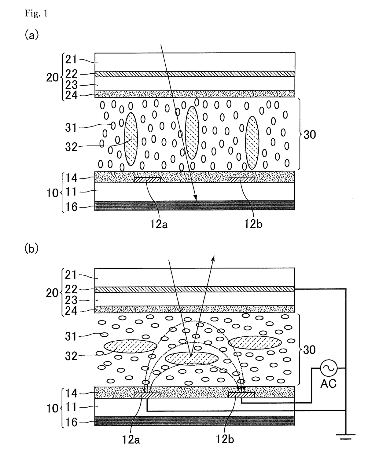
Examples
embodiment 1
[0041]An optical modulator of Embodiment 1 constitutes a reflective display device that provides display by utilizing reflection of light (external light) incident on the device from the outside of the device. The optical modulator provides black display with no voltage applied and provides white display or half-tone display (gray-scale display) with voltage applied. The optical modulator of Embodiment 1 includes pixels arranged in a matrix form and is configured to be switchable between the black display and the half-tone or white display in each pixel.
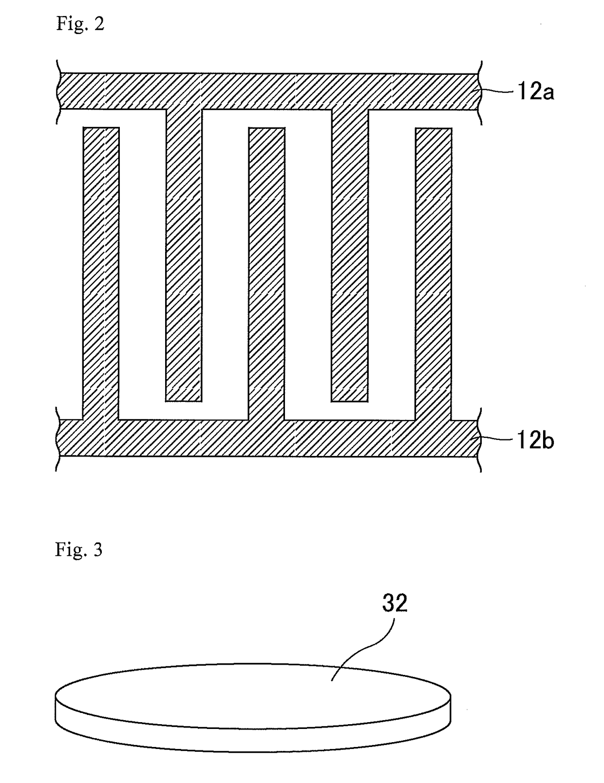
[0042]The overall configuration of the optical modulator of Embodiment 1 is described with reference to FIGS. 1(a) and 1(b) and FIG. 2. FIGS. 1(a) and 1(b) are schematic cross-sectional views of the optical modulator of Embodiment 1; FIG. 1(a) illustrates a voltage-off state and FIG. 1(b) illustrates a voltage-on state. FIG. 2 is a schematic plan view of an electrode structure provided in the optical modulator of Embodiment 1.
[0043]T...
embodiment 2
[0079]An optical modulator of Embodiment 2 constitutes a transmissive display device utilizing light from a light source to provide display. The optical modulator provides white display with no voltage applied and provides black display with voltage applied. Differences from Embodiment 1 are mainly described below.
[0080]FIGS. 6(a) and 6(b) are each a schematic cross-sectional view of an optical modulator of Embodiment 2; FIG. 6(a) illustrates a voltage-off state and FIG. 6(b) illustrates a voltage-on state. As illustrated in FIGS. 6(a) and 6(b), the optical modulator of Embodiment 2 includes a light source (backlight) 40 on the back surface side of the first substrate 10. The liquid crystal layer 30 serving as an optical modulation layer controls transmission and reflection of light emitted by the light source 40. Thus, the optical modulator of Embodiment 2 is structurally different from the optical modulator of Embodiment 1 in that it includes the light source 40 and does not inclu...
embodiment 3
[0086]An optical modulator of Embodiment 3 has a similar configuration to the optical modulator of Embodiment 1, except that the electrode structure of the first substrate was changed from the IPS electrode structure to the fringe field switching (FFS) electrode structure. The FFS electrode structure can reduce short circuits between the paired electrodes disposed in the first substrate. The FFS electrode structure can also prevent, with its planar electrode, influence of external static electricity on the optical modulator.
[0087]FIG. 7 is a schematic perspective view of an electrode structure in an optical modulator of Embodiment 3. As illustrated in FIG. 7, the optical modulator of Embodiment 3 includes, in the first substrate 10, a planar first electrode 112a and a second electrode 112b including parallel electrode slits (parts where no electrode is formed) are stacked with a dielectric layer (insulating film) 113 in between. The second electrode 112b having a planar shape includ...
PUM
| Property | Measurement | Unit |
|---|---|---|
| dielectric constant | aaaaa | aaaaa |
| surface energy | aaaaa | aaaaa |
| surface energy | aaaaa | aaaaa |
Abstract
Description
Claims
Application Information