Printed board and electronic apparatus

a technology of printed boards and electronic devices, applied in the direction of printed circuit components, printed circuit manufacturing, printed circuit applications, etc., can solve the problems of reducing the insulation resistance of printed boards, corroding of front surfaces of printed boards, and not saying that background-art printed boards have satisfactory resistance, so as to improve the resistance to a high-temperature high-humidity environmen

Inactive Publication Date: 2004-12-30
TOHOKU PIONEER CORP
View PDF4 Cites 5 Cited by
  • Summary
  • Abstract
  • Description
  • Claims
  • Application Information

AI Technical Summary

Benefits of technology

0047] As described above, the printed board 10 according to the embodiment includes an electrically insulating board 2 having one surface on which electronic parts will be mounted, and the other surface on which a conductor layer 14 made of an electrically conducting pattern is formed and covered with a resist layer 16 and/or an ink layer 17 each made of an electrically insulating solid pattern. Accordingly, a printed board improved in resistance to a high-temperature high-humidity environment can be obtained without necessity of extra cost and time.
0048] The orga...

Problems solved by technology

For this reason, it cannot be said that the background-art printed board has satisfactory resistance to a high-temperature high-humidity environment because water may go into the printed board through the exposed through-holes and lands.
There is hence a possibility that the front surface of the printed board may be corroded due to oxidization, or the insulation resistance of the pri...

Method used


Image

  • Printed board and electronic apparatus
  • Printed board and electronic apparatus
  • Printed board and electronic apparatus

Examples


Embodiment Construction

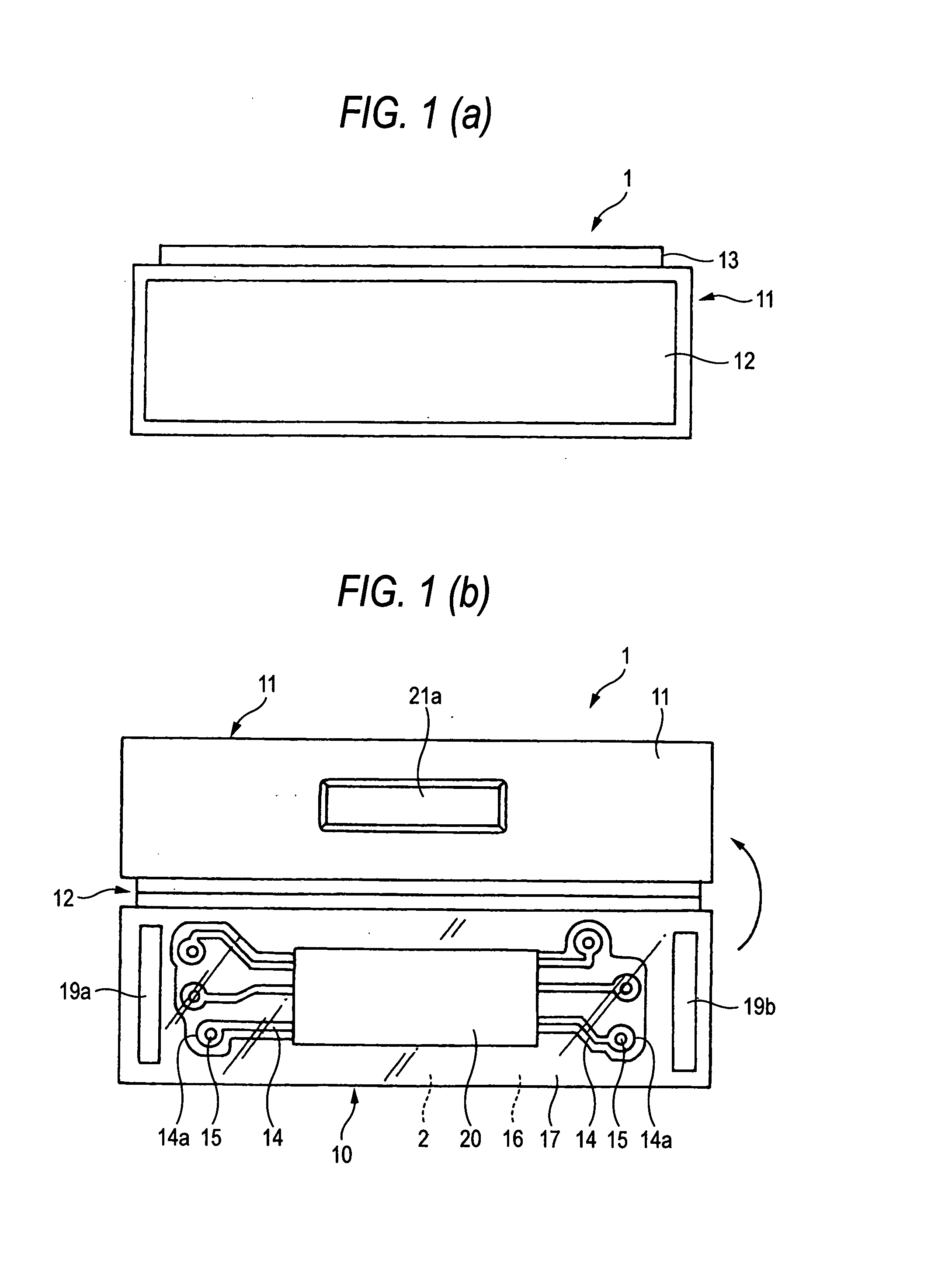
[0039] A result of comparison in a high-temperature high-humidity test between Example of an organic EL panel device using the printed board according to the embodiment and Comparative Example of an organic EL panel device using a printed board without a solid pattern of an ink layer will be described below.

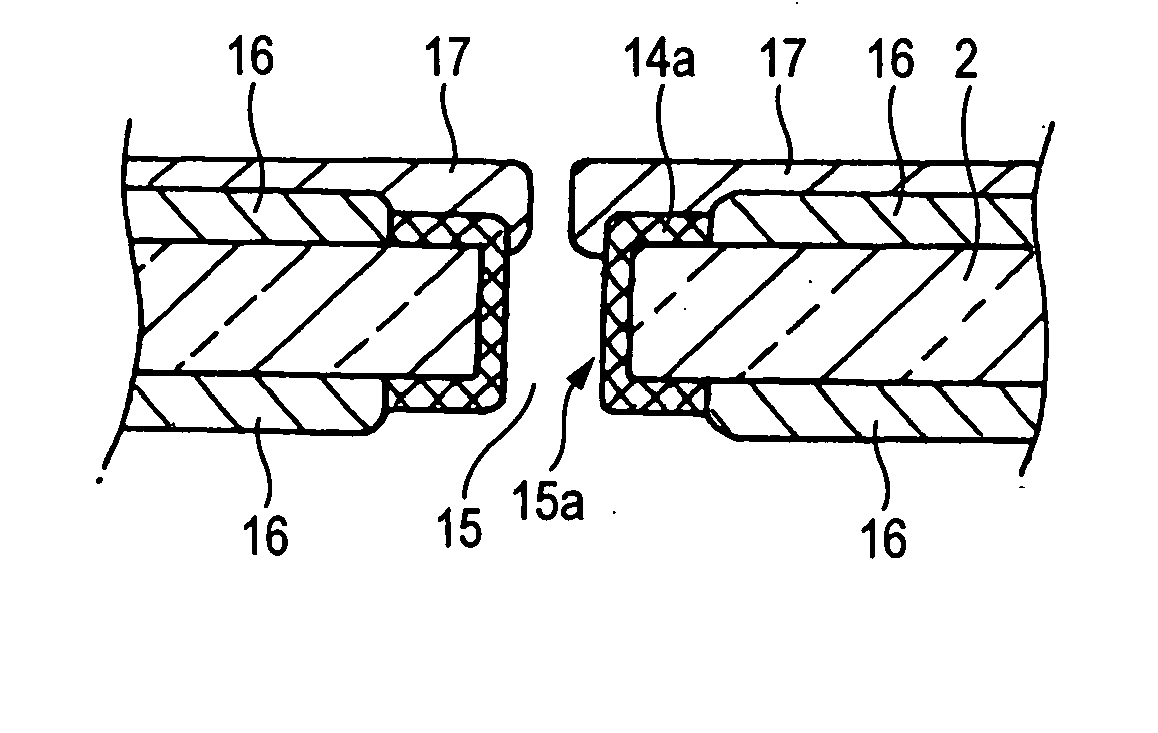
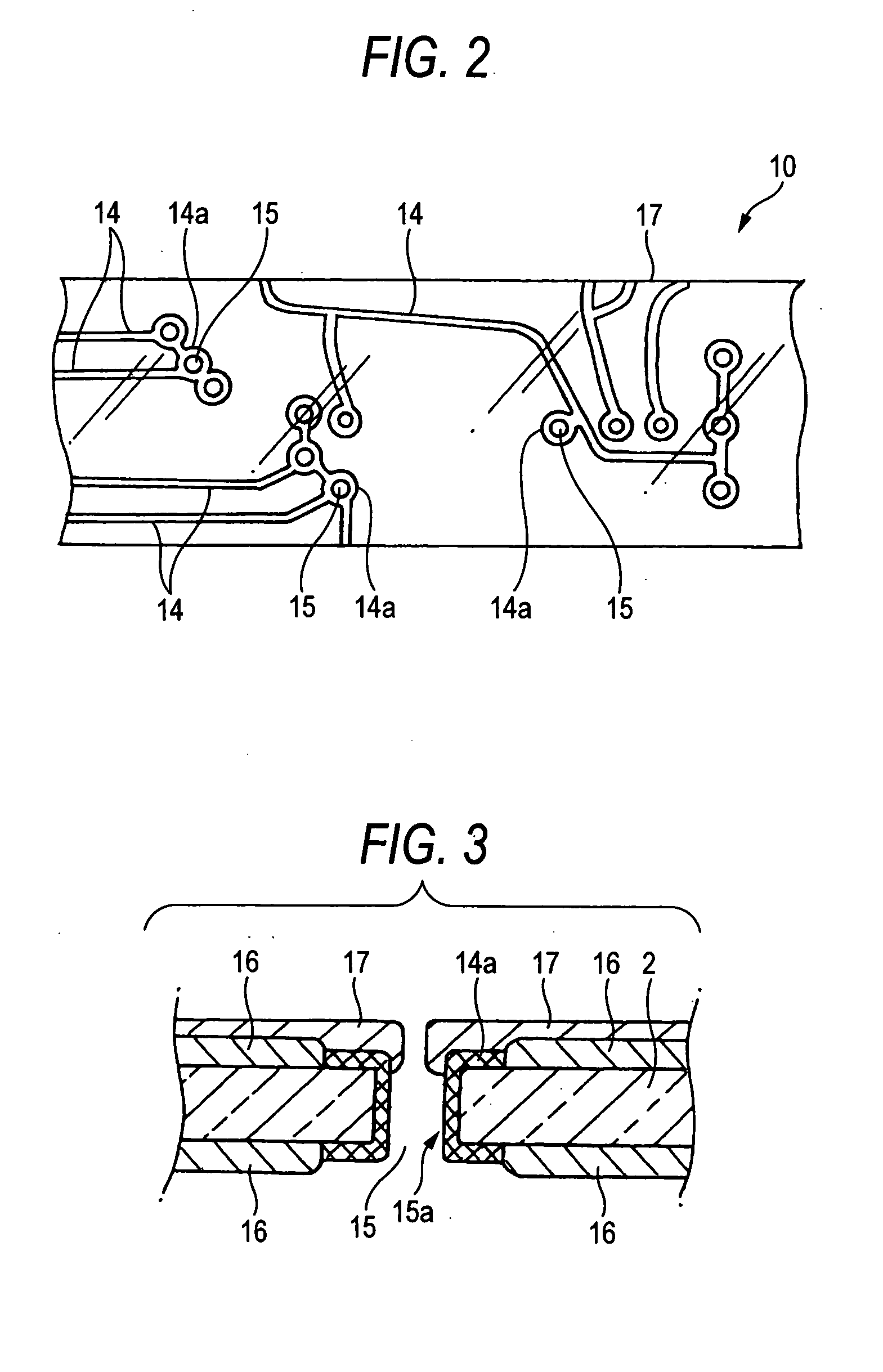
[0040] The organic EL panel device according to Comparative Example had the same structure as that in FIGS. 1A and 1B except that the solid pattern of the ink layer was not formed on the front surface of the printed board by silk-screen printing. Two identical samples each of which was provided as the organic EL panel device according to Comparative Example were put in a test furnace in the condition that the housing of each sample was closed so that the planar portion and the printed board faced each other while the display panel of each sample faced sideways. The environment in the furnace was set at a temperature of 85 .C and humidity of 85%. Then, a current was applied to eac...


PUM


Abstract

A printed board includes an electrically insulating board, a conductor layer made of an electrically conducting pattern, and at least one of a resist layer and an ink layer, each made of an electrically insulating solid pattern. The electrically insulating board has one surface on which electronic parts will be mounted, and the other surface on which the conductor layer is formed and covered with at least one of the resist layer and the ink layer. An organic EL display device includes the printed board, and a housing having a planar structure. The surface on which the conductor layer of the printed board is covered with at least one of the resist layer and the ink layer, each made of the electronically insulating solid pattern is arranged so as to face a planar portion of the housing having the planar structure.

Description

[0001] 1. Filed of the Invention[0002] The present invention relates to a printed board and an electronic apparatus.[0003] 2. Description of the Related Art[0004] Generally, electronic parts or the like constituting an electronic apparatus are mounted on a printed board. The printed board has an electrically insulating board which is made of a glass epoxy material or the like and which has one surface on which electronic parts will be mounted, and the other surface on which a conductor layer made of a conductor pattern of a circuit is formed by means of etching a sheet of copper foil or the like. The printed board further has through-holes which are formed in the electrically insulating board so that an inner wall of each through-hole is covered with a conductor by which conductors provided on the front and rear surfaces of the electrically insulating board are connected to each other so that the electronic parts can be electrically connected to the conductor layer.[0005] Lands for ...

Claims


Application Information

Patent Timeline
IPC IPC(8): H01L27/32H05K3/00H05K3/28
CPCH01L27/32H05K3/0094H05K3/28H05K2201/0195H10K59/00
Inventor TOGASHI, MASATO
Owner TOHOKU PIONEER CORP
Why Eureka
Try Eureka