CMOS differential buffer circuit

US20050035819A1Active Publication Date: 2005-02-17TEXAS INSTR INC

Image

  • CMOS differential buffer circuit
  • CMOS differential buffer circuit
  • CMOS differential buffer circuit

Examples


Embodiment Construction

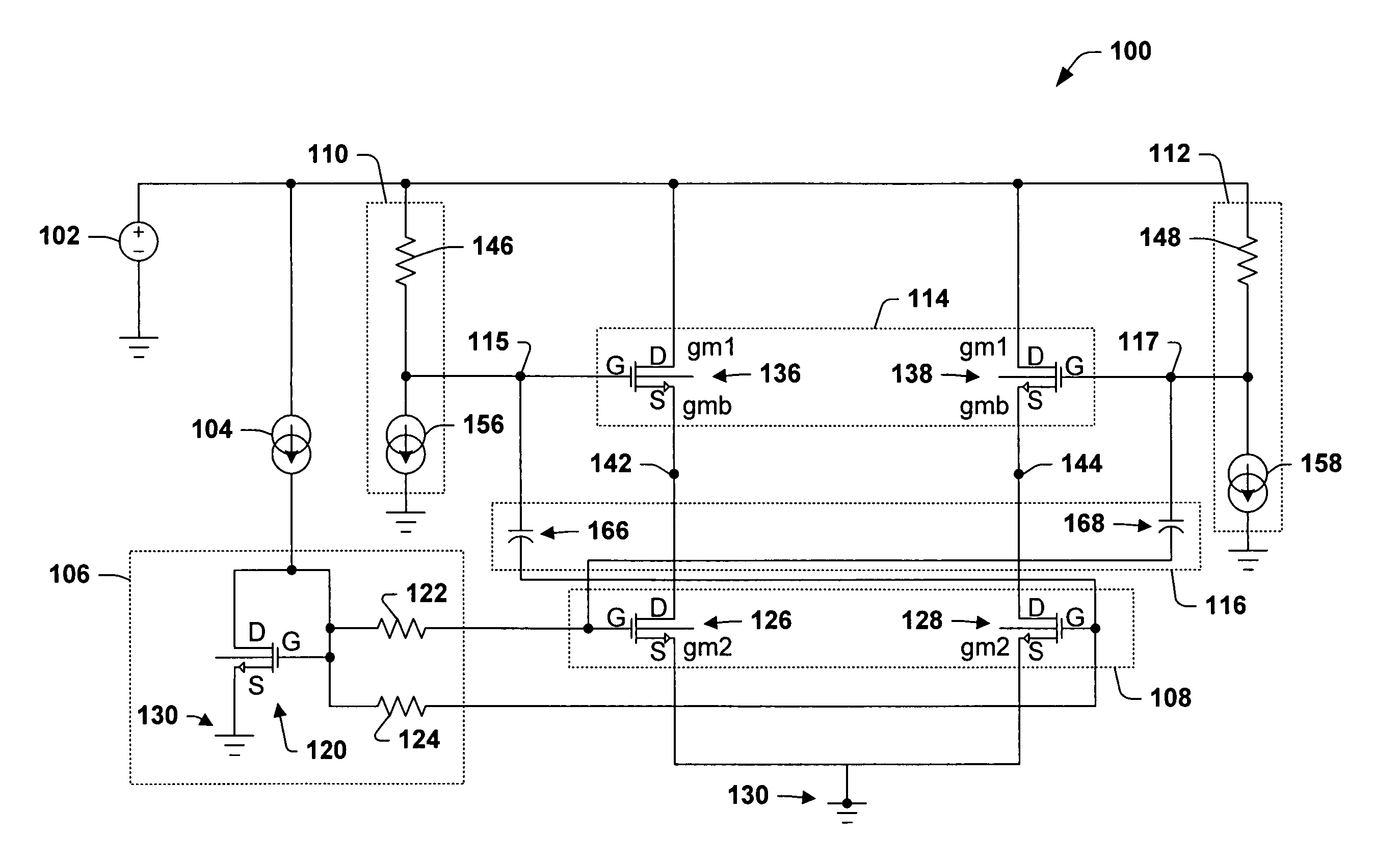
[0015] One or more aspects of the present invention are described with reference to the drawings, wherein like reference numerals are generally utilized to refer to like elements throughout, and wherein the various structures are not necessarily drawn to scale. In the following description, for purposes of explanation, numerous specific details are set forth in order to provide a thorough understanding of one or more aspects of the present invention. It may be evident, however, that one or more aspects of the present invention may be practiced with a lesser degree of these specific details. In other instances, well-known structures and devices are shown in block diagram form in order to facilitate describing one or more aspects of the present invention.

[0016] The present invention pertains to a MOS type differential buffer circuit. The buffer proposed herein utilizes capacitive coupling to apply small AC signals to an amplifying current source to mitigate attenuation owing to body ...


PUM


Abstract

The present invention pertains to a MOS type differential buffer circuit. The buffer proposed herein utilizes capacitive coupling to apply small AC signals to an amplifying current source to mitigate attenuation owing to body effect and output impedance, among other things, in an associated follower component. The proposed circuit does not, however, promote an increase in current and / or power dissipation. Additionally, the circuit allows a desired gain to be achieved while maintaining a relatively constant output impedance, compared to a simple differential source follower.

Description

RELATED APPLICATION [0001] This application claims priority to provisional application Ser. No. 60 / 494,174 filed Aug. 11, 2003, which is entitled “CMOS Differential Buffer Circuit”.FIELD OF INVENTION [0002] The present invention relates generally to buffer circuits, and more particularly to a CMOS differential buffer circuit wherein signal attenuation is mitigated via small signal AC capacitive coupling. BACKGROUND OF THE INVENTION [0003] A source follower is often used as a voltage buffer to drive subsequent circuits with a relatively low source impedance, especially in high-frequency applications. Voltage buffer circuits have a high input impedance and a low output impedance so that they can be utilized to drive subsequent circuits which have lower impedances than that which an input circuit without a buffer can drive. As such, the buffer can be put in-between the load circuits and input circuits so that the buffer feeds required current to the load circuits. However, complimentar...

Claims


Application Information

Patent Timeline
17 Feb 2005
Publication
US20050035819A1
IPC
H03F3/45
CPC
H03F3/45183; H03F2200/294; H03F2203/45644; H03F2203/45564; H03F2203/45632; H03F2200/372
Inventors
GHARPUREY, RANJIT