Tiled electronic display structure

a technology of electronic display and tiling, which is applied in the direction of identification means, tubes with screens, instruments, etc., can solve the problems of limiting the size of display devices that can be manufactured, not being able to meet the need for large-area displays, and not having a clear solution

Inactive Publication Date: 2005-04-14
MEC MANAGEMENT LLC +1
View PDF99 Cites 124 Cited by
  • Summary
  • Abstract
  • Description
  • Claims
  • Application Information

AI Technical Summary

Benefits of technology

[0022] According to another aspect of the invention, this circuitry also compensates for

Problems solved by technology

No clear solution is apparent in the market place.
There are fundamental technical issues that impose scaling-laws and limit the size of displays that can be manufactured.
These fundamental limitations are one reason why a technical solution that meets the need for large-area displays has not been achieved.
One measure of the complexity of a display device is its total number of pixels.
Increased complexity typically is accompanied by added costs.
The underlying cause of this empiric

Method used


Image

  • Tiled electronic display structure
  • Tiled electronic display structure
  • Tiled electronic display structure

Examples


Embodiment Construction

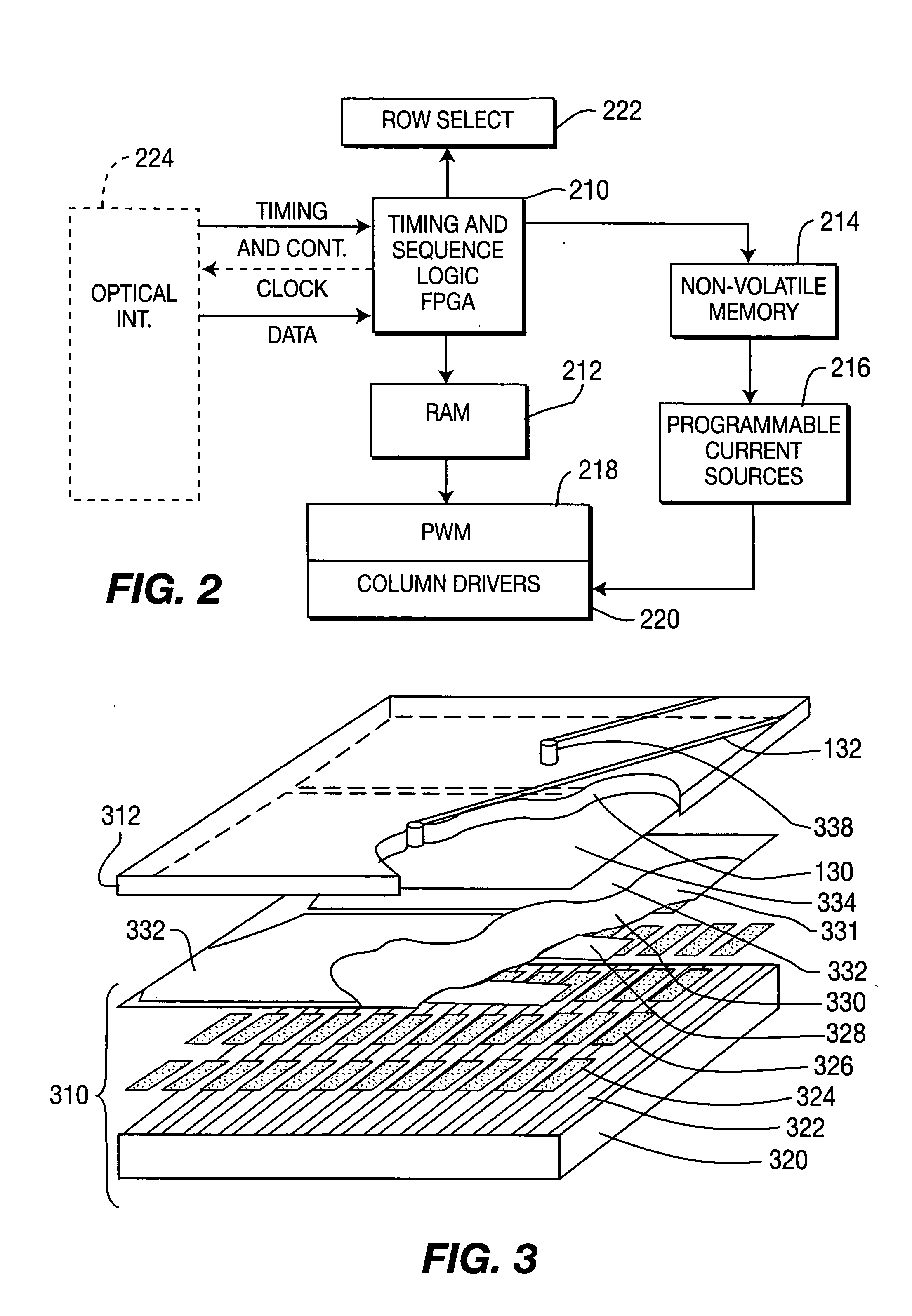
[0070] The invention is described in terms of exemplary embodiments which are illustrated in the drawing figures. The drawing figures are not to scale. Indeed, dimensions of the drawing figures are exaggerated to aid in the description of the invention. Although the invention is described in terms of an optical light emitting diode (OLED) display device, it is contemplated that it may be practiced with other emissive display technologies such as electroluminescent, light emitting diode (LED) or plasma technology; or with reflective display technologies such as Bistable, Reflective Cholesteric (BRC) liquid crystal technology.

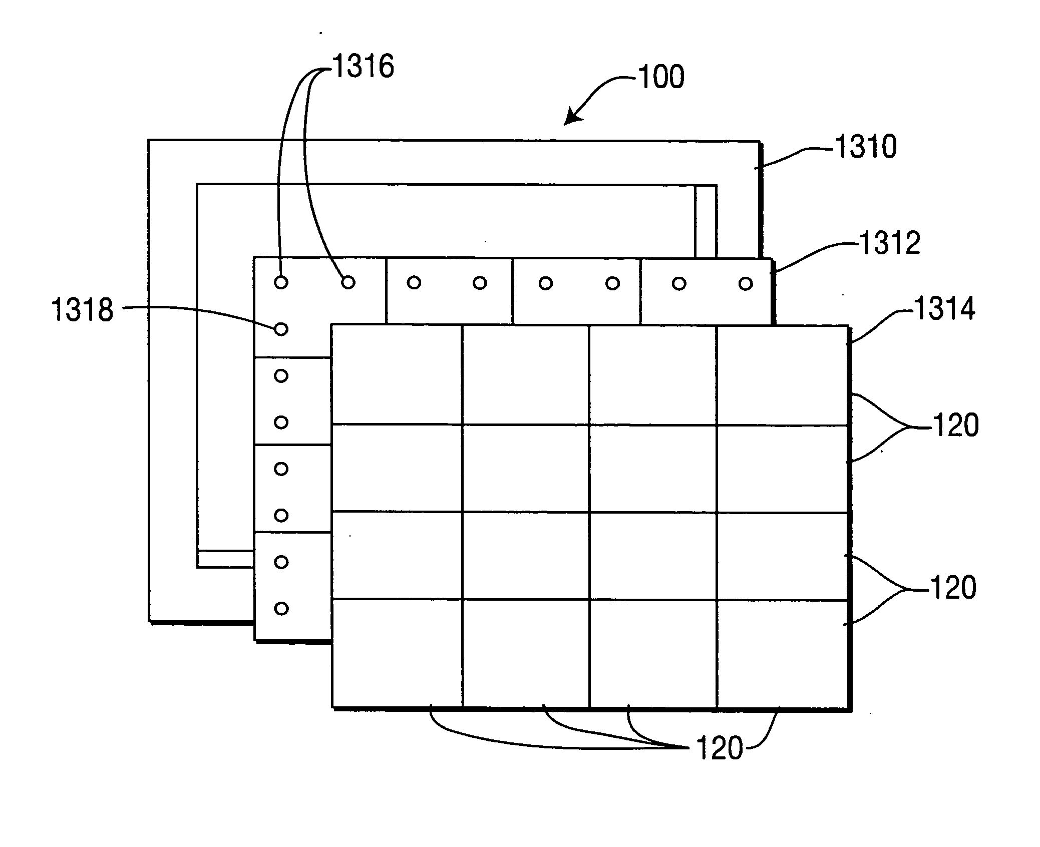
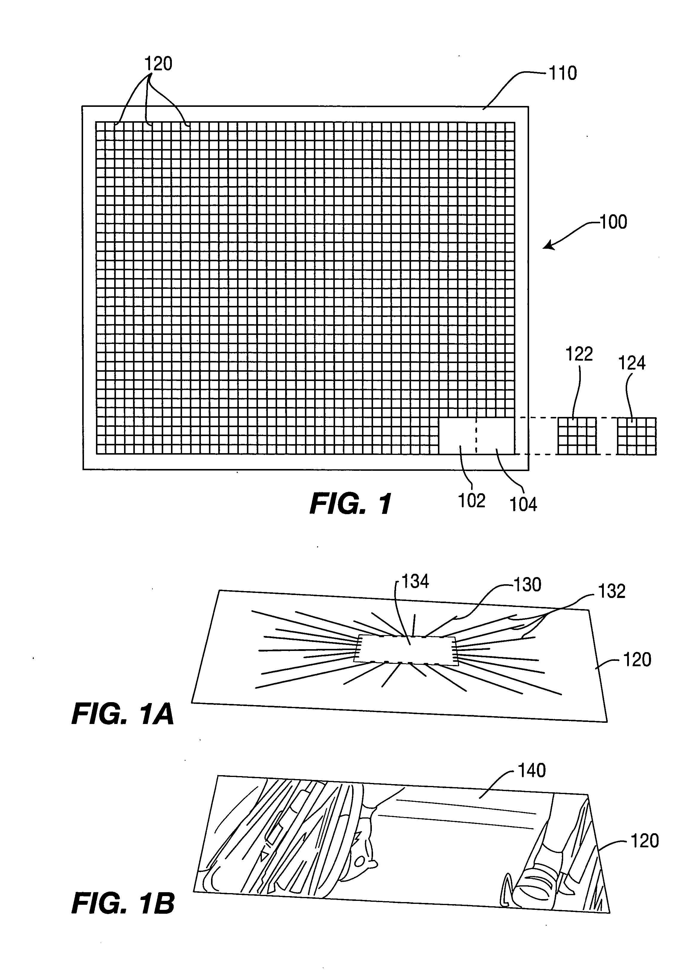
[0071]FIG. 1 is a front plan view of a partially assembled large-area display 100 according to the present invention. The display 100 is a tiled display in which emissive or reflective elements, on which the image pixels are formed, are built as relatively small arrays on tiles 120 and assembled into a frame to produce the large-area display having a large numbe...


PUM


Abstract

A tiled display device is formed from display tiles having picture element (pixel) positions defined up to the edge of the tiles. Each tile includes a memory which stores display data, and pixel driving circuitry which controls the scanning and illumination of the pixels on the tile. The tiles are formed in two parts, an electronics section and a display section. Each of these parts includes connecting pads which cover several pixel positions. Each connecting pad makes an electrical connection to only one row electrode or column electrode. The connecting pads on the display section are electrically connected and physically joined to corresponding connecting pads on the electronics section to form a complete tile.

Description

[0001] This patent application is a divisional of U.S. application No. 09 / 250,324, filed Feb. 16, 1999 which claims the benefit of priority from U.S. Provisional application No. 60 / 074,922 filed Feb. 17, 1998.BACKGROUND OF THE INVENTION [0002] The present invention concerns electronic display devices and, in particular, large-area display devices which are formed as an array of tiled display devices. [0003] There is an unmet need for large-area flat displays. No clear solution is apparent in the market place. This unmet need is becoming increasingly critical since the advancement of information results in increasing amounts of data to be displayed. A solution for large-area displays is needed to serve as the human interface for conveying information from sensors, computers, data bases, cameras etc. in this information dominated age. Many critical applications demand large-area displays: [0004] Home theater applications [0005] Applications that require multiple viewers [0006] Applica...

Claims


Application Information

Patent Timeline
IPC IPC(8): G02F1/1333G02F1/1347G02F1/1335G09F9/30G09G3/20G09G3/22G09G3/30G09G3/32H01J29/74H01J29/76H01J31/12H01J31/15H01L25/16H01L27/15H01L27/32H01L51/50H01L51/52H05B33/12
CPCG02F1/13336G02F1/133512H01L2924/0002G09G3/3208G09G2300/026G09G2300/0426G09G2320/048H01L25/167H01L27/156H01L27/3293H01L51/5262H01L51/5281H01L2924/09701H01L2924/00H10K59/18H10K50/85H10K50/86
Inventor MATTHIES, DENNIS LEESTEWART, ROGER GREENATHERTON, JAMES HAROLDBECHIS, DENNIS J.BUSTA, HEINZ H.SHEN, ZILAN
Owner MEC MANAGEMENT LLC
Why Eureka
Try Eureka