

Silicide resistor in BEOL layer of semiconductor device and method
a technology of resistor and semiconductor, applied in the direction of resistors, semiconductor devices, electrical equipment, etc., can solve the problems of high thermal requirements for activation annealing of dopants (excess of 900° c.) in the formation of polysilicon devices, too large structures for typical chip wiring or back, etc., to achieve a few additional manufacturing steps
- Summary
- Abstract
- Description
- Claims
- Application Information
AI Technical Summary
Benefits of technology
Problems solved by technology
Method used
Image

Examples
Embodiment Construction
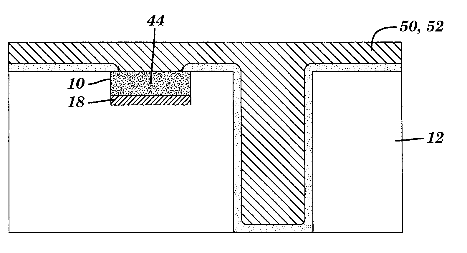
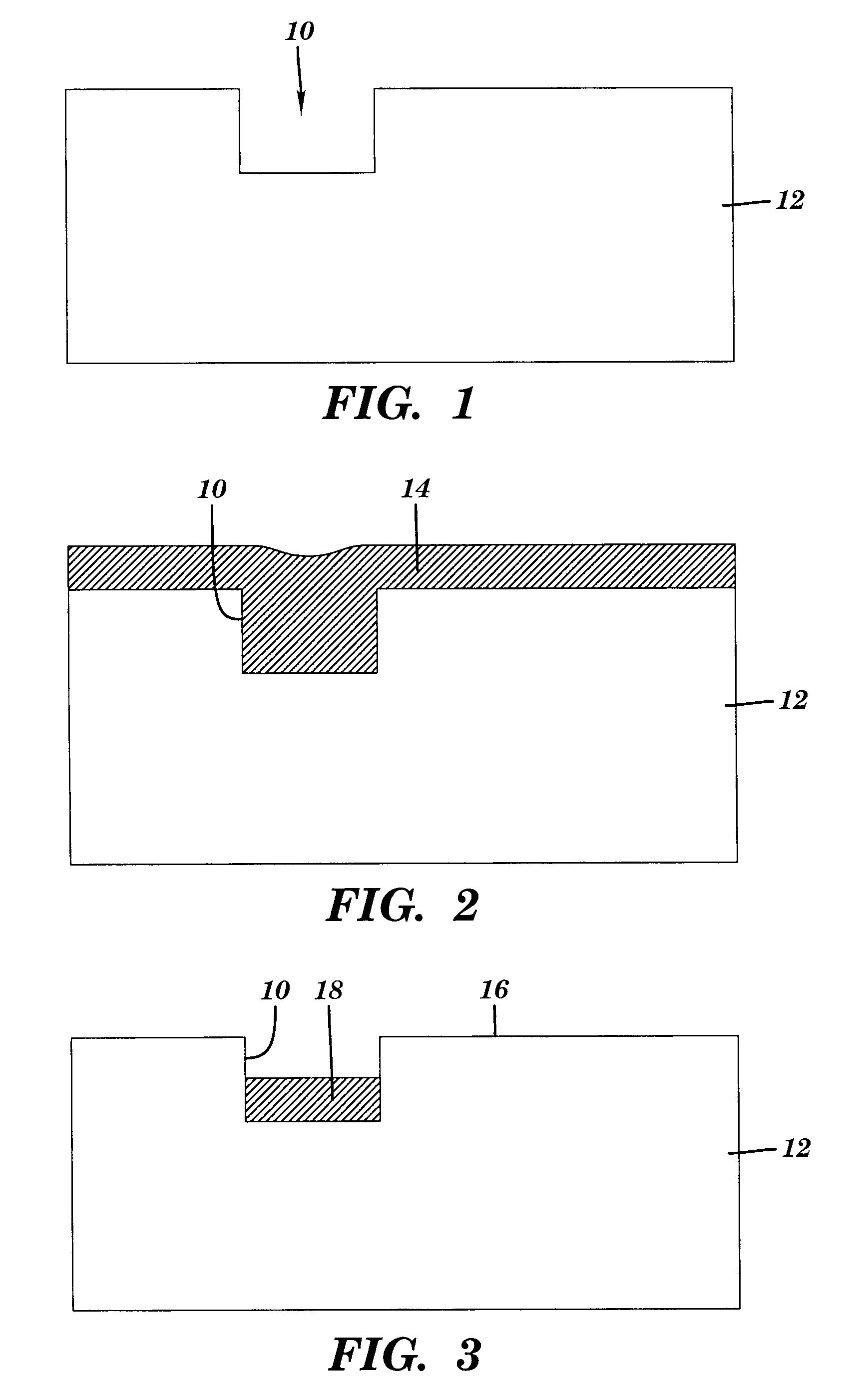
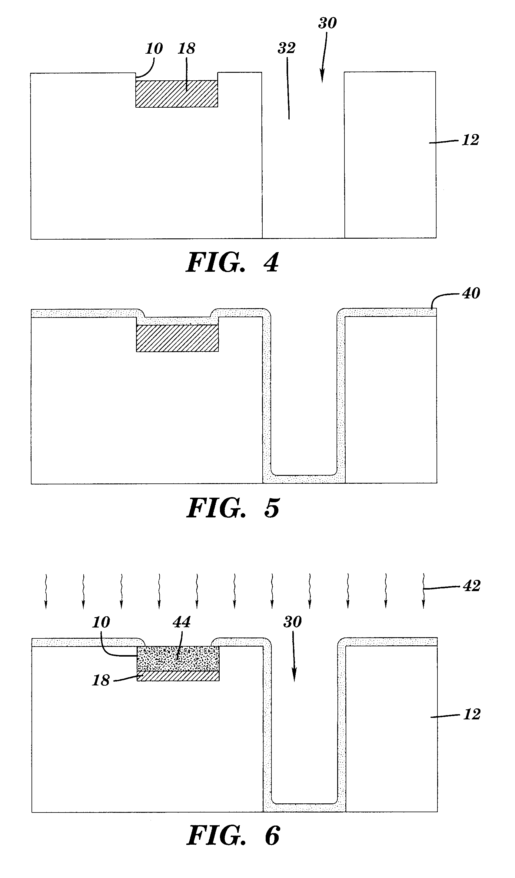
[0017] With reference to the accompanying drawings, FIG. 1 illustrates a first step of a method for generating a silicide resistor 100 (FIG. 8) according to the invention. In FIG. 1, a trough 10 is formed in an inter-layer dielectric (ILD) layer 12 of a plurality of back-end-of-line (BEOL) layers (not shown for clarity—above and / or below ILD layer 12) such as via layer and / or metal layers. Formation of trough 10 may be made by patterning and etching in a conventional fashion. ILD layer 12 may be any now known or later developed dielectric layer used with BEOL layer such as silicon dioxide SiO2 (hereinafter “oxide”), SiLK® available from Dow Chemical, boron doped oxide, a high-k dielectric, chemical vapor deposited (CVD) low-k material, FSG, FTEOS or other dielectric known in the industry. ILD layer 12 may be positioned above another dielectric layer (not shown) that may include wiring therein. It should be recognized, however, that ILD layer 12 may be any BEOL layer, e.g., it could ...
PUM
 Abstract
Description
Claims
Application Information