Level shifter having automatic delay adjusting function

a level shifter and automatic delay technology, applied in the field of level shifters, can solve the problems of disadvantageous ill balanced delay times and complicating the whole circuit, and achieve the effect of effective rising delay time, and reducing rise delay tim

Inactive Publication Date: 2005-11-24
SOCIONEXT INC
View PDF5 Cites 44 Cited by
  • Summary
  • Abstract
  • Description
  • Claims
  • Application Information

AI Technical Summary

Benefits of technology

[0014] In one aspect of the level shifter having an automatic delay adjusting function, the automatic delay adjusting circuit compensatively increases the quantity of a current flowing to the output terminal when the rise delay time of the output signal output from the output terminal is longer than the fall delay time.
[0019] In another aspect of the level shifter having an automatic delay adjusting function, the automatic delay adjusting circuit compensatively reduces lowering of a voltage on the side of the input terminal of the level shifting unit or a voltage on the side of the output terminal of the level shifting unit when the rise delay time of the output signal output from the output terminal is longer than the fall delay time.
[0025] For example, in the case where the rise delay time and the fall delay time of an output signal from an output terminal are set to be substantially the same time when a voltage level is shifted to be higher, if the voltage level is shifted to be lower due to change of first and second power voltages, the rise delay time becomes longer than the fall delay time. However, in the level shifter having the automatic delay adjusting function of this invention, the automatic delay adjusting circuit automatically corrects imbalance between the delay times even in such a case, so that an input signal can be level-shifted always with appropriate delay characteristics regardless of the values of the power voltages attained before and after the level shift.
[0026] For example, in this invention, although the rise delay time of the output signal from the level shifting unit tends to be increased in such a case, the automatic delay adjusting circuit makes a large current flow to the output terminal so as to compensate the voltage increase of the output signal, and hence, the rise delay time is reduced to be balanced with the fall delay time. In particular, in this invention, when it is necessary to compensate the delay times because the imbalance between the rise and fall delay times is large, namely, merely when the second power voltage is lower than the first power voltage, the P-type transistor is turned on so as to allow a large current to flow to the output terminal. Furthermore, in this invention, a large current is allowed to flow to the output terminal by using the current mirror circuit, the rise delay time can be effectively reduced. In addition, in this invention, the second N-type transistor is turned off when the output signal from the output terminal has undergone a transition to H level, and therefore, a steady state current flowing from the current mirror circuit can be cut so as to reduce the power consumption.
[0027] Moreover, in this invention, when the rise delay time of the output signal becomes longer than the fall delay time, the fall of the input signal to the level shifting unit is slowed so as to increase the fall delay time of the output signal, or the rise of the output signal from the level shifting unit is shortened so as to reduce the rise delay time of the output signal. Thus, the balance between the rise delay time and the fall delay time can be satisfactorily kept.

Problems solved by technology

In the conventional level shifter, however, when the internal voltage level VDD1 and the external voltage level VDD2 are changed, a large time difference is caused between the rise delay time tpLH and the fall delay time tpHL of the output signal, and therefore, these delay times are disadvantageously ill balanced.
Accordingly, the number of wires is increased, resulting in disadvantageously complicating the whole circuit.

Method used


Image

  • Level shifter having automatic delay adjusting function
  • Level shifter having automatic delay adjusting function
  • Level shifter having automatic delay adjusting function

Examples


embodiment 1

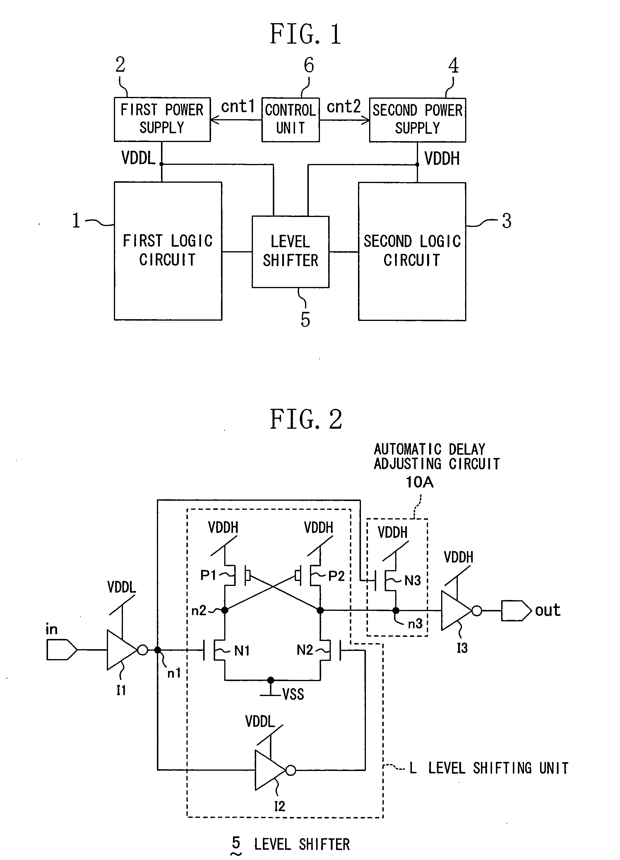
[0046]FIG. 1 is a block diagram of a system using a level shifter having an automatic delay adjusting function according to Embodiment 1 of the invention.

[0047] In FIG. 1, a reference numeral 1 denotes a first logic circuit, a reference numeral 2 denotes a first power supply for supplying a first power voltage VDDL, a reference numeral 3 denotes a second logic circuit, a reference numeral 4 denotes a second power supply for supplying a second power voltage VDDH, a reference numeral 5 denotes a level shifter having an automatic delay adjusting function disposed between the first logic circuit 1 and the second logic circuit 3, and a reference numeral 6 denotes a control unit for changing the first and second power voltages VDDL and VDDH of the first and second power supplies 2 and 4.

[0048] The first power voltage VDDL is supplied to the first logic circuit 1 by the first power supply 2, and the second power voltage VDDH is supplied to the second logic circuit 3 by the second power s...

embodiment 2

[0064] A level shifter having an automatic delay adjusting function according to Embodiment 2 of the invention will now be described with reference to the accompanying drawings.

[0065]FIG. 4 is a circuit diagram of the level shifter having the automatic delay adjusting function of this embodiment. The level shifter of FIG. 4 has a basic configuration substantially the same as that of the level shifter of FIG. 2 but is different in an automatic delay adjusting circuit 10B including a P-type MOS transistor P3 in addition to the N-type MOS transistor N3.

[0066] In the automatic delay adjusting circuit 10B, the source of the N-type MOS transistor N3 is connected to the output terminal out and the gate thereof is connected to the input node n1 of the level shifting unit L. Furthermore, in the P-type MOS transistor P3, the drain thereof is connected to the drain of the N-type MOS transistor N3, the first power voltage VDDL is supplied to the source thereof and the second power voltage VDD...

embodiment 3

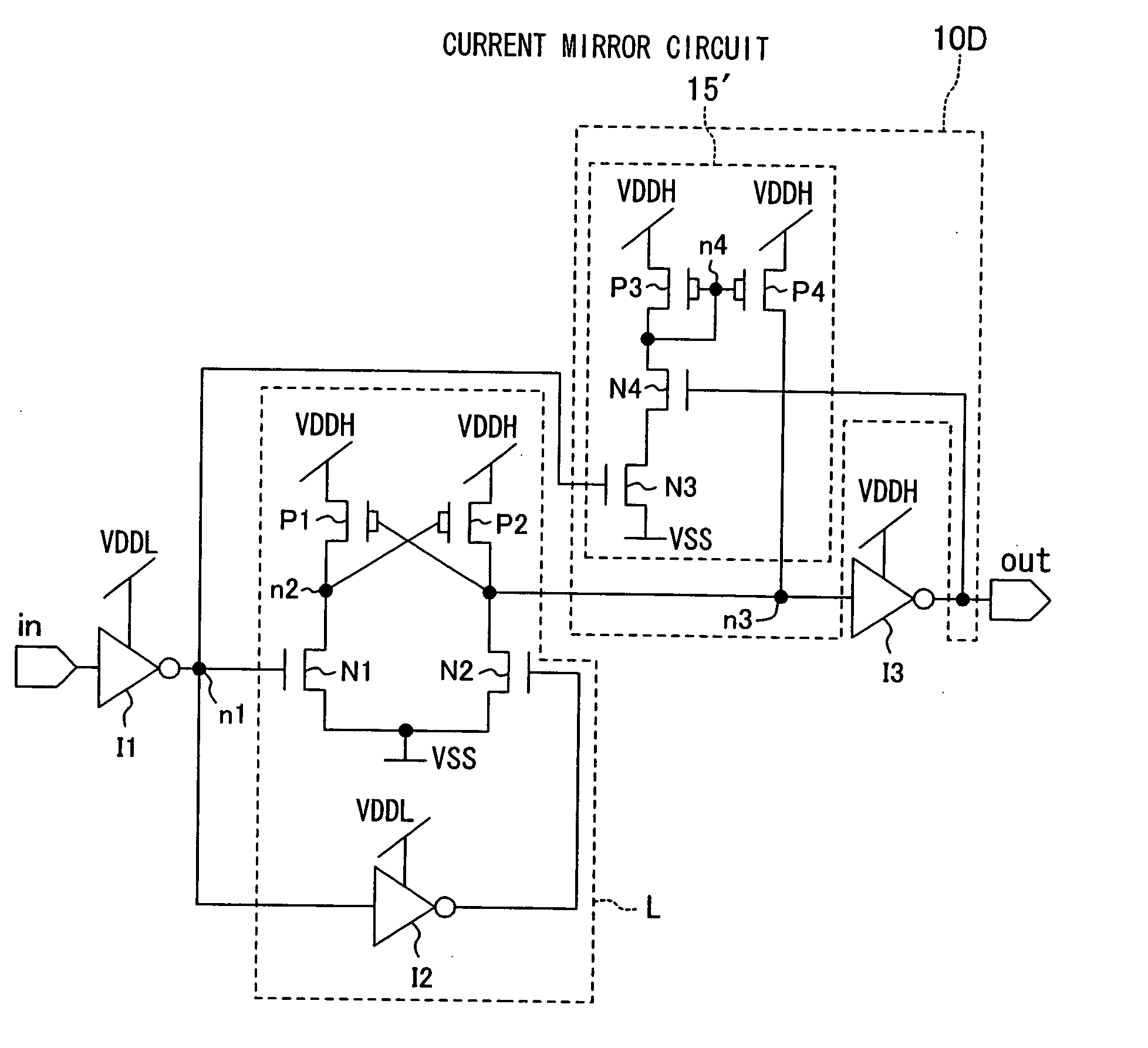
[0071] A level shifter having an automatic delay adjusting function according to Embodiment 3 of the invention will now be described with reference to the accompanying drawing.

[0072]FIG. 6 is a circuit diagram of the level shifter having the automatic delay adjusting function of this embodiment. The level shifter of FIG. 6 includes a current mirror circuit 15 as an automatic delay adjusting circuit 10C.

[0073] The current mirror circuit 15 includes a first N-type MOS transistor N3 and first and second P-type MOS transistors P3 and P4. In the N-type MOS transistor N3, the ground voltage VSS is supplied to the source thereof, the drain thereof is connected to the gates of the first and second P-type MOS transistors P3 and P4 and the gate thereof is connected to the input node n1 of the level shifting unit L. Also, in the first P-type MOS transistor P3, the drain thereof is connected to the drain of the first N-type MOS transistor N3 and the second power voltage VDDH is supplied to th...


PUM


Abstract

In a level shifter, in the case where the amplitude voltage of an input signal (i.e., a first power voltage VDDL) input to an input terminal is changed to be higher and the amplitude voltage of an output signal (i.e., a second power voltage VDDH) output from an output terminal is changed to be lower, a fall delay time of the signal output from the output terminal tends to be longer than a rise delay time of the signal. However, an inverted input signal obtained by an inverter is input to a level shifting unit and also to the gate of an N-type transistor, and therefore, the N-type transistor is turned on at the fall of the input signal input to the input terminal, so as to supply a current based on the second power voltage VDDH to an output node of the level shifting unit for assisting the shift into H level performed in the level shifting unit. Accordingly, even when at least one of the amplitude voltage of the input signal and the amplitude voltage of the output signal is changed, balance between the fall delay time characteristic and the rise delay time characteristic of the output signal can be satisfactorily kept.

Description

BACKGROUND OF THE INVENTION [0001] The present invention relates to a level shifter disposed between two logic circuits respectively driven by different power voltages for shifting the voltage level of an output signal of one of the logic circuits to supply the shifted voltage to the other logic circuit. [0002] Recently, portable equipment to which power is supplied from batteries have been widely spread, and in order to elongate the driving time of the batteries, it is earnestly required to reduce the power consumption of a system used in such portable equipment. On the other hand, among these portable equipment, particularly cellular phones are required to have a large number of functions for, for example, e-mails, web browsing and games apart from its original communication function. Therefore, in a semiconductor integrated circuit included in such portable equipment, power voltages are changed in respective blocks therein in accordance with requested functions, so as to lower th...

Claims


Application Information

Patent Timeline
Patent Type & Authority Applications(United States)
IPC IPC(8): H03K19/0185H03K3/011H03K3/356H03K5/153H03L5/00
CPCH03K3/356113H03K3/011
Inventor ITO, MIWANAKANISHI, KAZUYUKIHIRATA, AKIOYAMAMOTO, HIROOHATSUDA, TSUGUYASU
Owner SOCIONEXT INC
Why Eureka
Try Eureka