Seal ring for mixed circuitry semiconductor devices

Active Publication Date: 2006-01-19
MICREL
View PDF5 Cites 18 Cited by
  • Summary
  • Abstract
  • Description
  • Claims
  • Application Information

AI Technical Summary

Benefits of technology

[0016] The present invention generally provides for a method and apparatus for selectively isolating peripheral seal rings of semico

Problems solved by technology

In other words, if a seal ring were tied to a higher potential, there is the possibility that if there are cracks or pinholes in the chip passivation layer over interconnect metal of a lower potential, then metal at a crack or pinhole would become a galvanic cell anode of very small area compared to the relatively large area of the ring—acting as a galvanic cell cathode—and rapid corrosion at the crack or pinhole could occur.
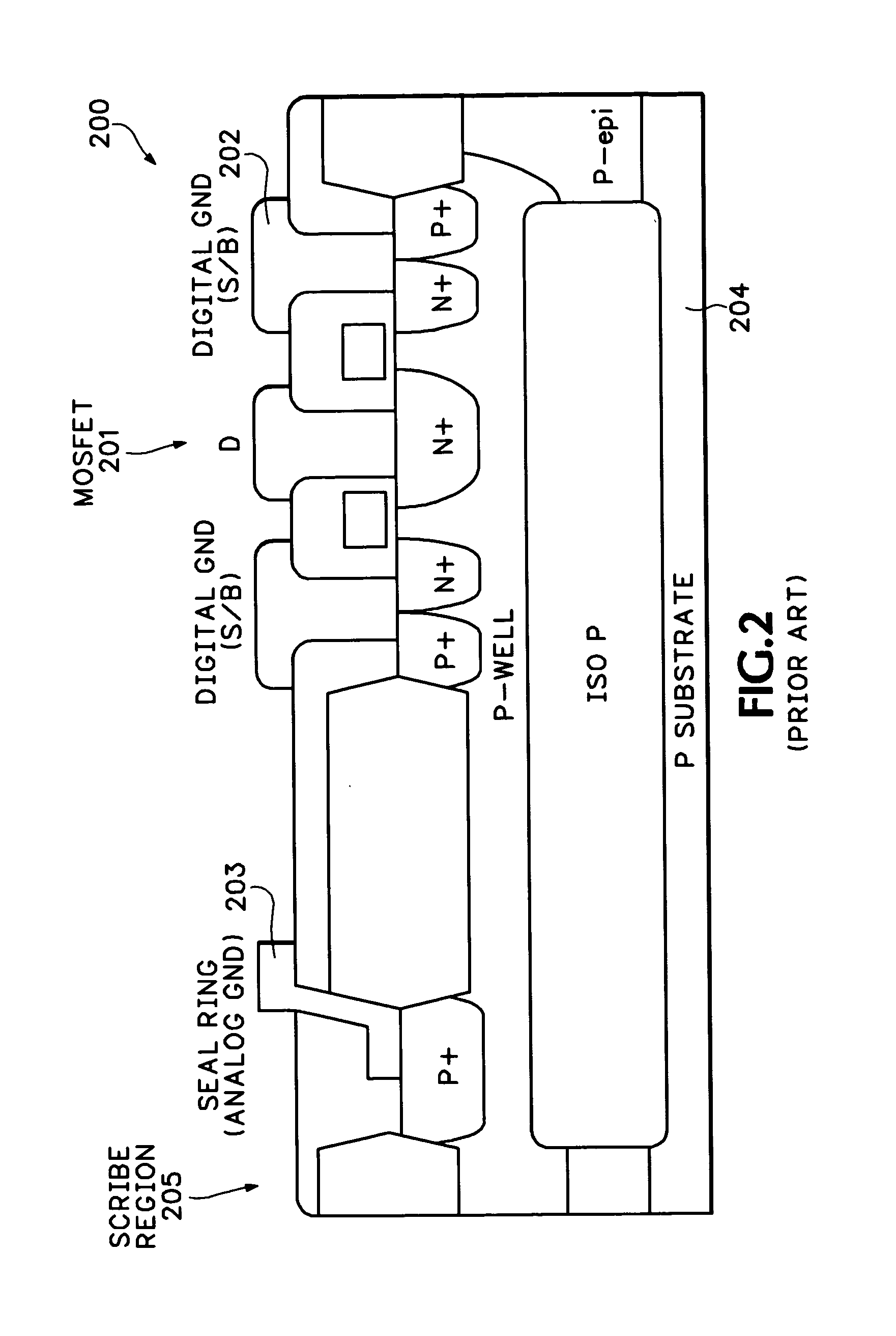
In these mixed analog-digital and analog-digital-power IC devices, since the seal ring conventionally completely encircles the chip core circuitry, one problem is that digital circuitry electrical noise can affect operation of analog circuitry. FIG. 1 (Prior Art) is a simplified, schematic, block diagram illustrating such a die 80 (FIG. 1 is also in common assignee's U.S. Pat. No. 6,395,591 (McCormack et al.) as FIG._4).
It is known that digital circuits and power circuits are in general electrically noisy.
On the other hand, analog circuits are generally both quiet and sensitive to electrical noise.
In mixed signal integrated circuits such as illustrated by FIG. 1, noisy power and digital core circuit blocks adjacent to the seal ring can couple noise into the quiet analog circuit block via the seal rings ohmic contact to the substrate, disrupting analog operations.

Method used


Image

  • Seal ring for mixed circuitry semiconductor devices
  • Seal ring for mixed circuitry semiconductor devices
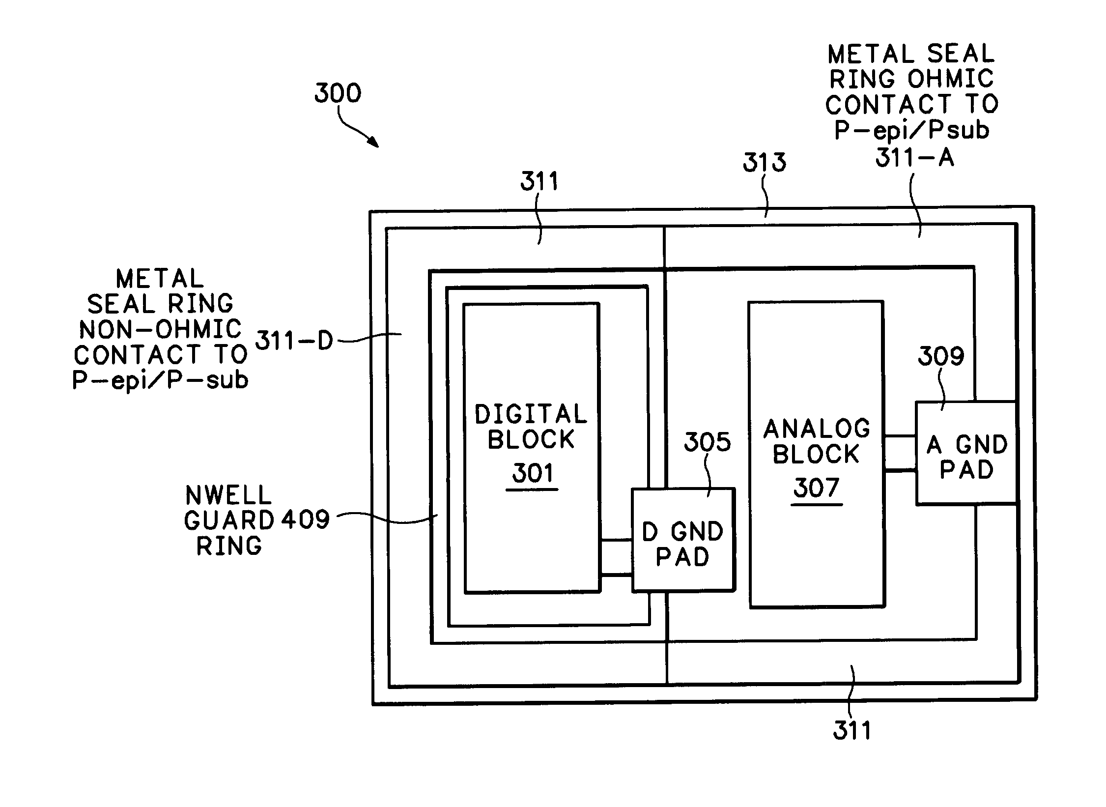
  • Seal ring for mixed circuitry semiconductor devices

Examples


Embodiment Construction

[0026] The present invention is described with respect to exemplary embodiments. The exemplary embodiments are provided for enabling implementation and for explaining the best mode(s) of implementation currently known to the inventors. Specific implementations of the present invention may vary from said embodiments. No limitation on the scope of the invention, substantially defined by the Claims hereinafter, is intended by the details of these exemplary embodiments, nor should any be implied therefrom.

[0027] In general, in accordance with the present invention, selective seal ring isolation from the substrate and its electrical potential is provided in order to segregate noisy core circuitry from noise sensitive core circuitry in mixed signal semiconductor devices. Appropriate sections of a mixed use circuitry—analog, digital, power—chip are isolated selectively from the substrate through a non-ohmic contact, i.e., with a very high resistance or a junction barrier, to the substrate...


PUM


Abstract

In mixed-component, mixed-signal, semiconductor devices, selective seal ring isolation from the substrate and its electrical potential is provided in order to segregate noise sensitive circuitry from electrical noise generated by electrically noisy circuitry. Appropriate predetermined sections of such a mixed use chip are isolated from the substrate through a non-ohmic contact with the substrate without compromising reliability of the chip's isolation from scribe region contamination.

Description

(2) CROSS-REFERENCE TO RELATED APPLICATIONS [0001] Not applicable. (3) STATEMENT REGARDING FEDERALLY SPONSORED RESEARCH OR DEVELOPMENT [0002] Not applicable. (4) REFERENCE TO AN APPENDIX [0003] Not applicable. (5) BACKGROUND [0004] 1. Technical Field [0005] The technology described herein is generally related to the field of semiconductor devices and, more particularly, to seal rings for integrated circuit devices having core circuitry generating both analog and digital signals. [0006] 2. Description of Related Art [0007] Integrated circuit (IC) devices, each commonly having an area of less than one square inch, are fabricated simultaneously in multiples on a larger wafer, commonly having a cross-dimension of many inches. The individual IC devices, also known as “chips” or “die,” are segregated by “scribe lines” regions where the wafer can be sawed into individual chips once the fabrication is complete. Conventionally, surfaces of the chips are generally protected by the deposition ...

Claims


Application Information

Patent Timeline
IPC IPC(8): H01L29/00
CPCH01L21/761H01L21/765H01L21/823481H01L23/585H01L2924/0002H01L2924/00
InventorMALLIKARJUNASWAMY, SHEKARALTER, MARTIN
OwnerMICREL