

Semiconductor device with STI and its manufacture
a semiconductor device and semiconductor technology, applied in the direction of semiconductor devices, basic electric elements, electrical appliances, etc., can solve the problems of parasitic transistors turning on at a low threshold voltage, high integration of semiconductor devices, etc., to reduce mobility, suppress reverse narrow channel effects, and reduce the effect of hump
- Summary
- Abstract
- Description
- Claims
- Application Information
AI Technical Summary
Benefits of technology
Problems solved by technology
Method used
Image

Examples
Embodiment Construction
[0047] Embodiments of the invention will be described with reference to the accompanying drawings.
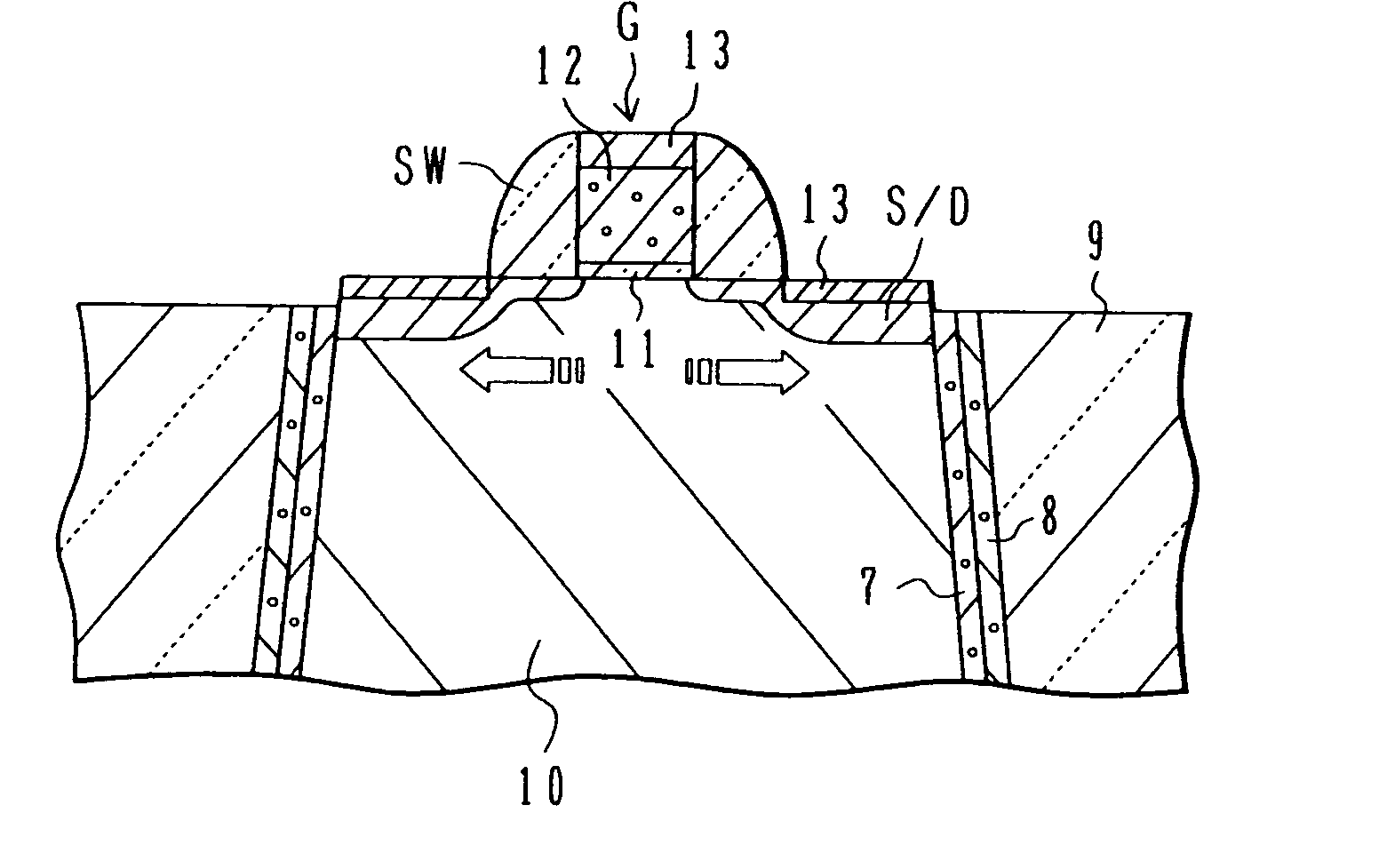
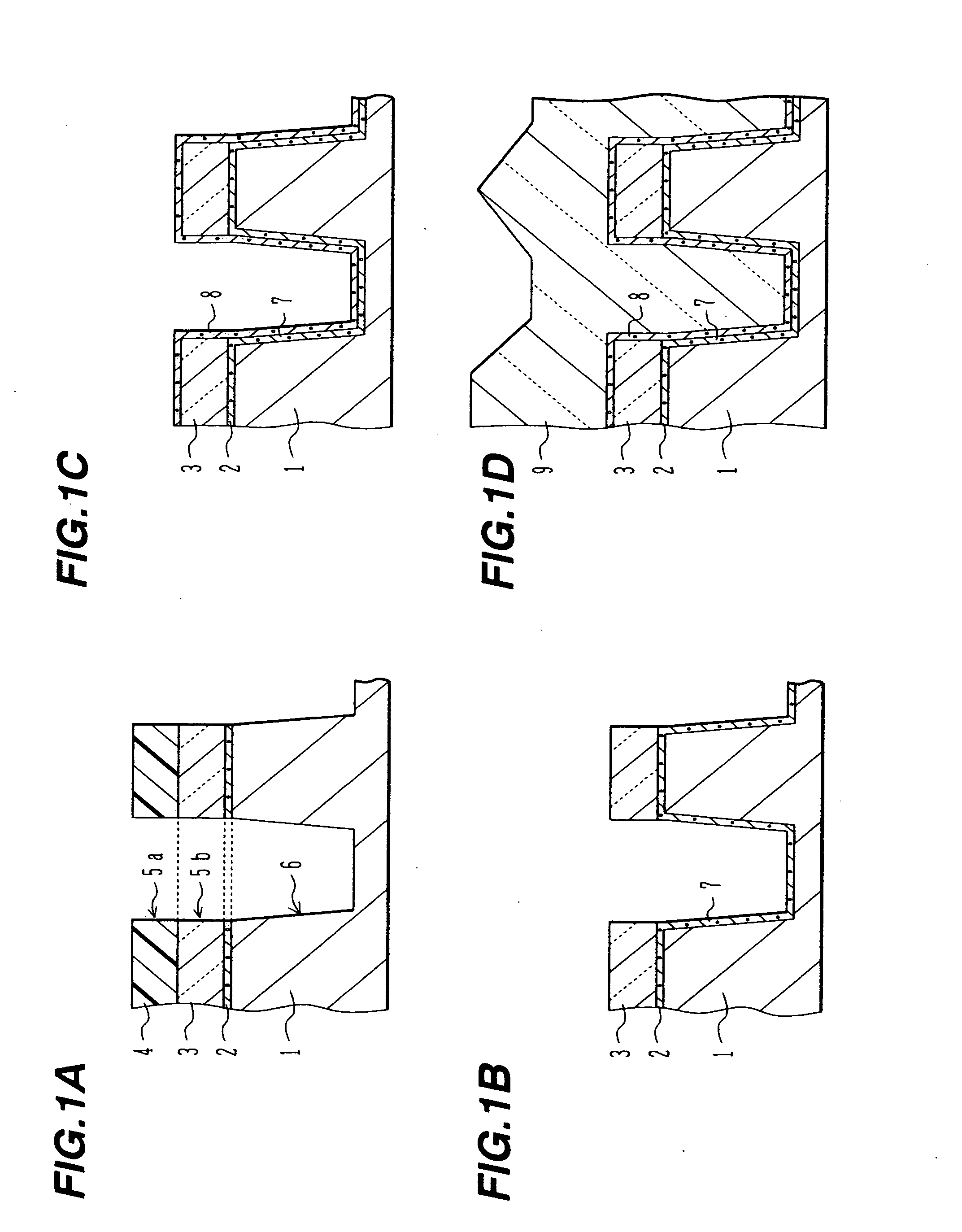
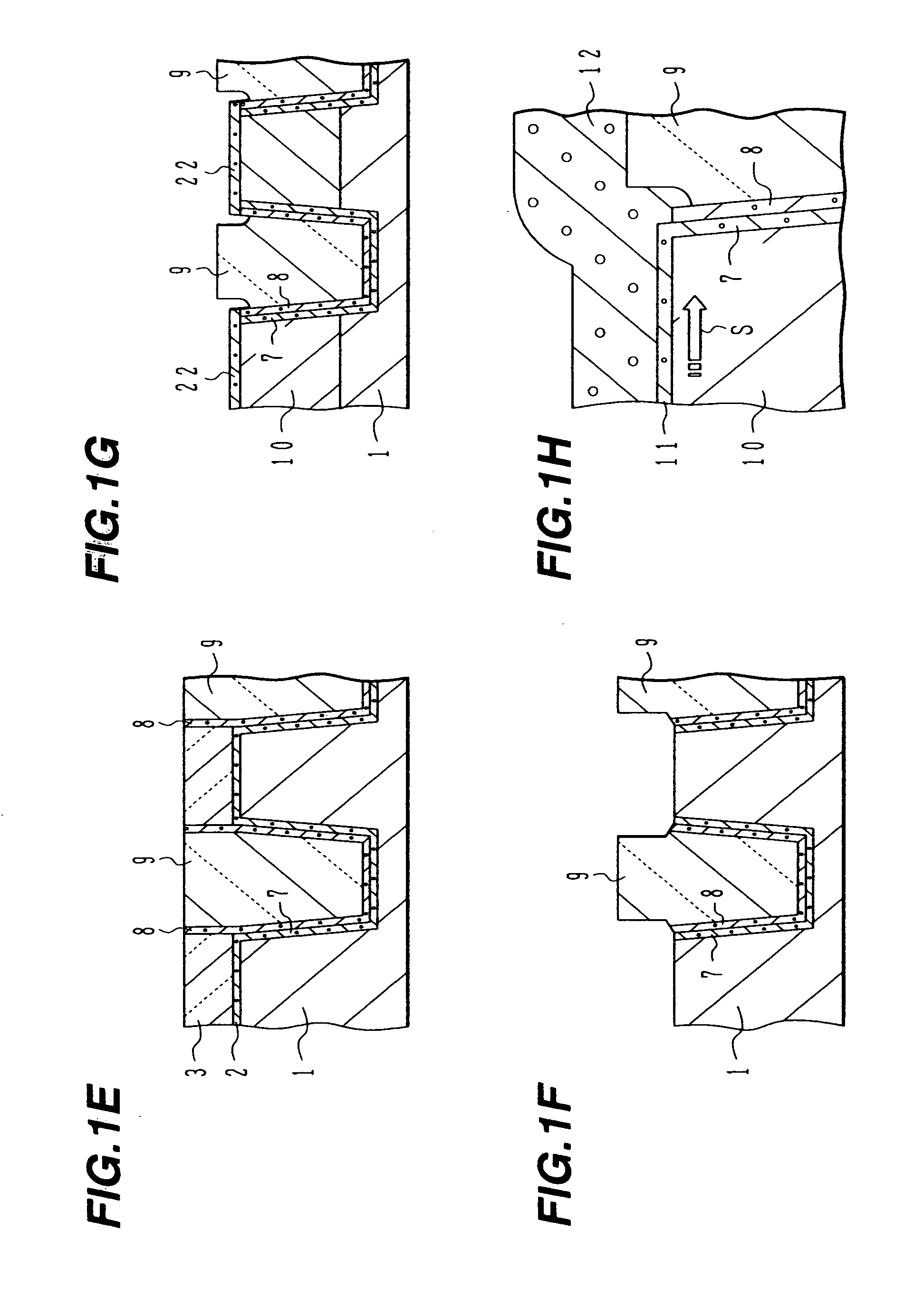
[0048]FIGS. 1A to 1H are schematic cross sectional views illustrating main processes of a method of manufacturing a semiconductor device according to an embodiment of the invention.
[0049] As shown in FIG. 1A, the surface of a silicon substrate 1 is thermally oxidized to form a silicon oxide film 2 having a thickness of 9 to 21 nm, e.g., 10 nm. On the silicon oxide film 2, a silicon nitride film 3 having a thickness of 100 to 150 nm is formed by low pressure (LP) chemical vapor deposition (CVD). For example, LPCVD is performed at a temperature of 700° C. by using SiCl2H2 and NH3 as source gas.
[0050] A resist film is coated on the silicon nitride film 3, exposed and developed to form a resist pattern 4. The resist pattern 4 has an opening or openings for defining an isolation region or regions and active regions (element regions) each surrounded by the isolation region. The width of an...
PUM
 Abstract
Description
Claims
Application Information