

Producing Method of Semiconductor Device
a technology of semiconductor devices and manufacturing methods, applied in semiconductor devices, electrical equipment, electric discharge tubes, etc., can solve the problems of thinning tendency and insufficient silc enduran
- Summary
- Abstract
- Description
- Claims
- Application Information
AI Technical Summary
Problems solved by technology
Method used
Image

Examples
Embodiment Construction
[0013] Next, preferable embodiments of the present invention will be described.
[0014] According to a preferable embodiment of the present invention, there is provided a producing method of a semiconductor device comprising a step of forming a tunnel insulating film of a flash device, comprising:
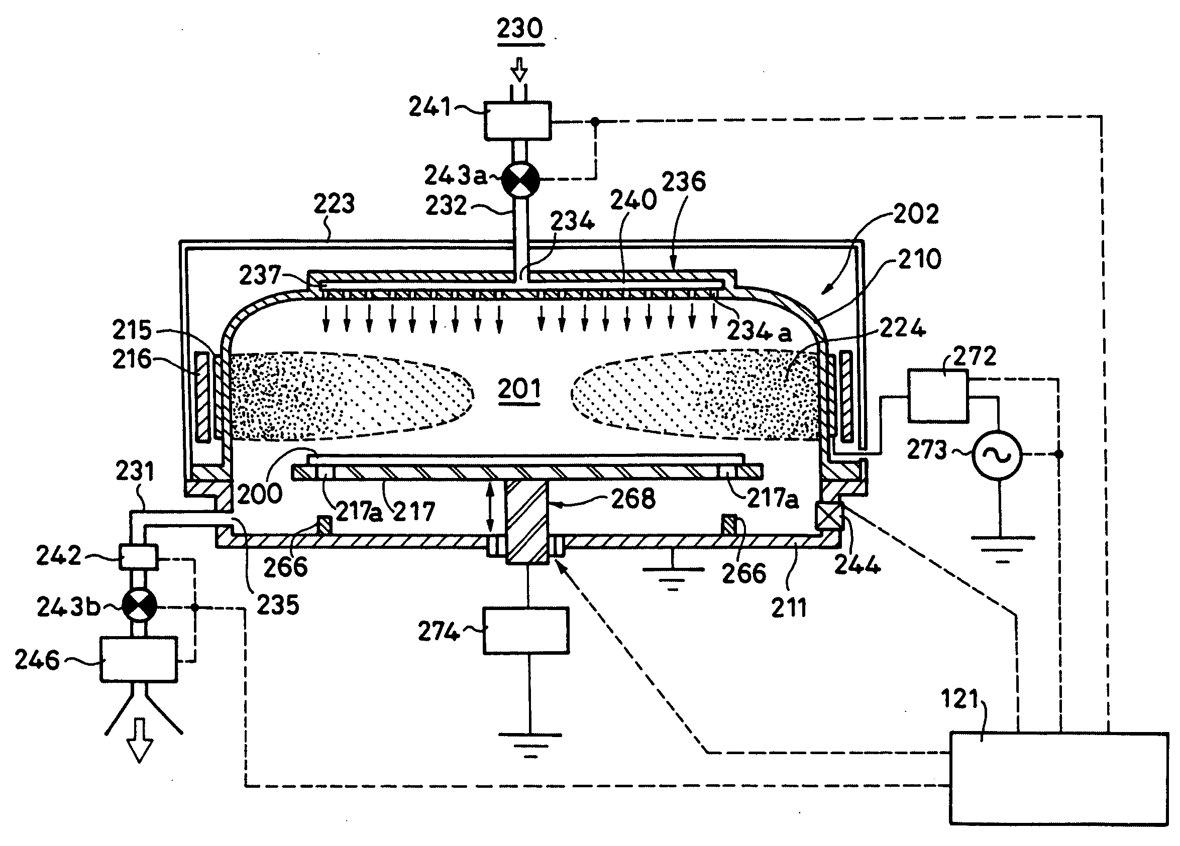
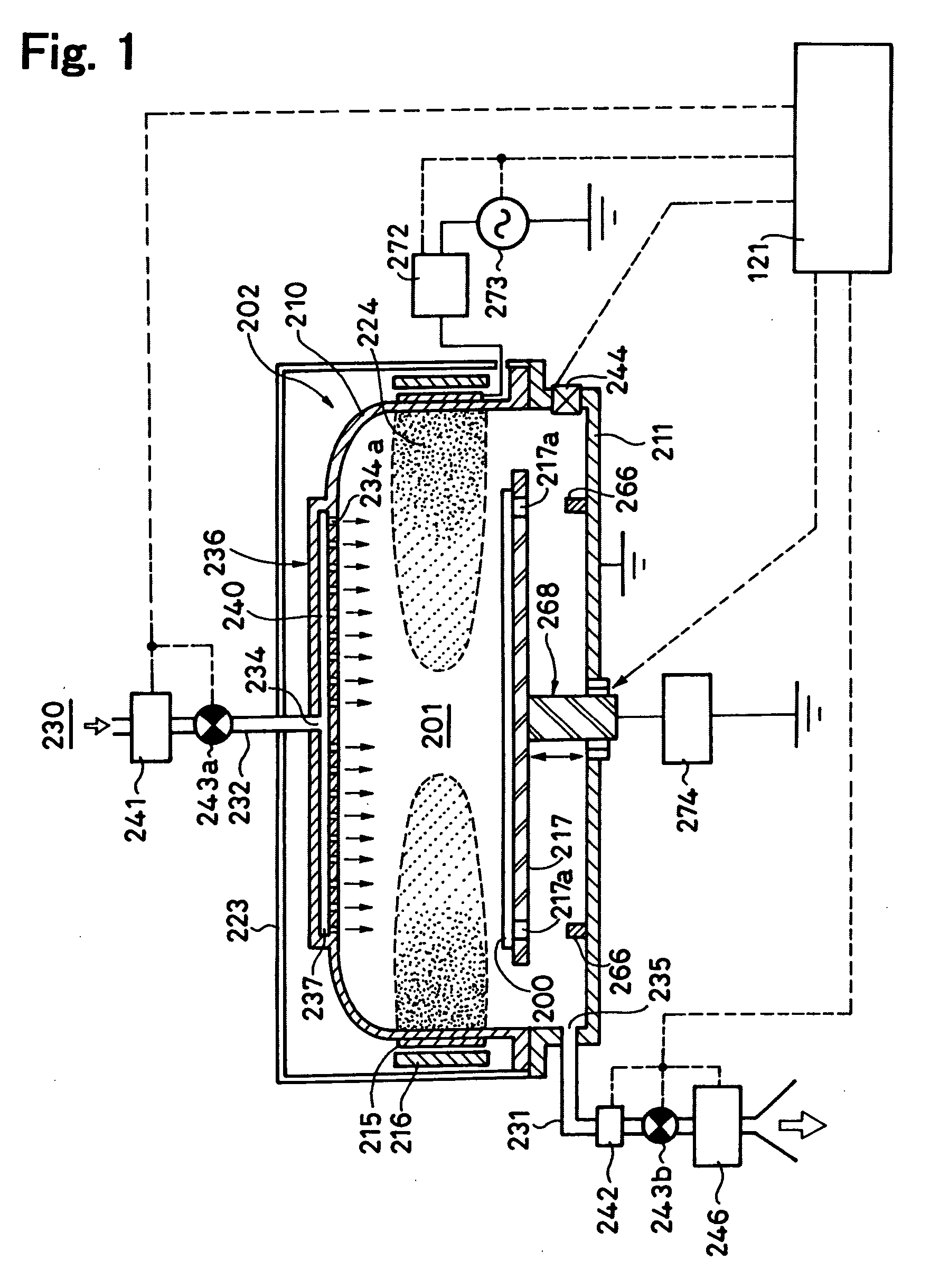
[0015] a first nitridation step of forming a first silicon oxynitride film by nitriding a silicon oxide film formed on a semiconductor silicon base by one of plasma nitridation and thermal nitridation, the plasma nitridation carrying out nitridation process by using a gas activated by plasma discharging a first gas including a first compound which has at least a nitrogen atom in a chemical formula thereof, and the thermal nitridation carrying out nitridation process using heat by using a second gas including a second compound which has at least a nitrogen atom in a chemical formula thereof, and
[0016] a second nitridation step of forming a second silicon oxynitride film by nitriding the fir...
PUM
 Abstract
Description
Claims
Application Information