Pixel and organic light emitting display device using the same

a technology of organic light, which is applied in the direction of instruments, static indicating devices, etc., can solve the problems of shortened charging duration of the threshold voltage of the driving transistor, non-uniform display, and inability to manufacture all transistors of the organic light emitting display device. achieve uniform luminance

Inactive Publication Date: 2011-04-28
SAMSUNG DISPLAY CO LTD
View PDF7 Cites 25 Cited by
  • Summary
  • Abstract
  • Description
  • Claims
  • Application Information

AI Technical Summary

Benefits of technology

[0030]As described above, according to embodiments of the present invention of a pixel and an organic light emitting display device using the same, it is possible to set a charging duration of a threshold voltage regardless of the width of a scan signal to thereby be applicable to high-speed driving. Further, in exemplary embodiments of the present invention, the threshold voltage of a driving

Problems solved by technology

Such an organic light emitting display device has an advantage in low power consumption, but a disadvantage in that the amount of current that flows to the organic light emitting diode varies depending on a threshold voltage variation (e.g., deviation) of the driving transistor included in each of the pixels, thereby causing display nonuniformity.
In fact, it may be impossible to manufacture

Method used


Image

  • Pixel and organic light emitting display device using the same
  • Pixel and organic light emitting display device using the same
  • Pixel and organic light emitting display device using the same

Examples


first embodiment

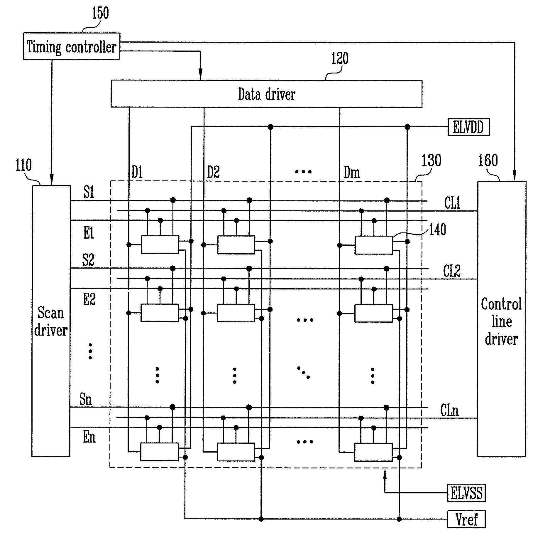
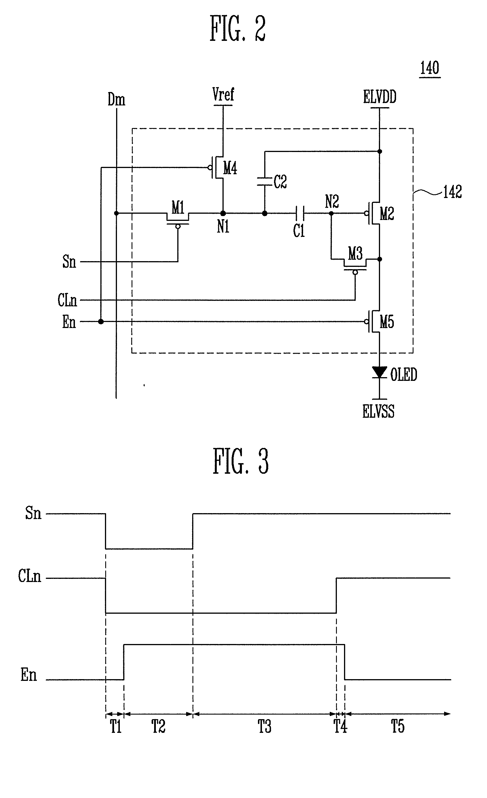
[0045]FIG. 2 is a circuit diagram showing a pixel shown in FIG. 1. In FIG. 2, a pixel connected to an n-th scan line Sn and an m-th data line Dm is shown for convenience of description.

[0046]Referring to FIG. 2, the pixel 140 includes an organic light emitting diode OLED and a pixel circuit 142 for controlling the amount of current supplied to the organic light emitting diode OLED.

[0047]The organic light emitting diode OLED generates light having a set or predetermined luminance to correspond to the amount of current supplied from the pixel circuit 142. For example, the organic light emitting diode OLED generates red, green, or blue light having the set or predetermined luminance to correspond to the amount of current supplied from the pixel circuit 142. An anode of the organic light emitting diode OLED is connected to the pixel circuit 142. A cathode of the organic light emitting diode OLED is connected to a power source of the second power ELVSS.

[0048]The pixel circuit 142 receive...

second embodiment

[0069]FIG. 4 is a diagram showing the pixel shown in FIG. 1. When FIG. 4 is described, the same components as those of FIG. 2 refer to the same reference numerals and a detailed description thereof will be omitted.

[0070]Referring to FIG. 4, the pixel 140 includes an organic light emitting diode OLED and a pixel circuit 142′ for controlling the amount of current supplied to the organic light emitting diode OLED. The organic light emitting diode OLED generates light having certain or predetermined luminance to correspond to the amount of current supplied from the pixel circuit 142′.

[0071]The pixel circuit 142′ receives the data signal when the scan signal is supplied to the scan line Sn and charges voltage corresponding to the threshold voltage of the second transistor M2 during the period when the control signal is supplied to the control line CLn. Compared to the pixel circuit 142 in FIG. 2, the second capacitor C2 is deleted from the pixel circuit 142′ and a sixth transistor M6, fo...


PUM


Abstract

A pixel and an organic light emitting device that can display an image having a desired luminance. The pixel includes an organic light emitting diode (OLED), first through third transistors, and a first capacitor. The OLED has a cathode electrode coupled to a second power source. The second transistor controls the current from a first power source to the OLED. The first capacitor has a first terminal coupled to a gate electrode of the second transistor. The first transistor is coupled between a second terminal of the first capacitor and a data line, and turns on when a scan signal is supplied to a scan line. The third transistor is coupled between the gate electrode and a second electrode of the second transistor, and turns on when a control signal is supplied to a control line. The third transistor remains turned on for a longer time than the first transistor.

Description

CROSS-REFERENCE TO RELATED APPLICATION[0001]This application claims priority to and the benefit of Korean Patent Application No. 10-2009-0101691, filed on Oct. 26, 2009, in the Korean Intellectual Property Office, the entire content of which is incorporated herein by reference.BACKGROUND[0002]1. Field[0003]Aspects of the present invention relate to a pixel and an organic light emitting display device using the same and, more particularly, to a pixel and an organic light emitting display device that can display an image having a desired luminance.[0004]2. Description of Related Art[0005]In recent years, various flat panel display devices capable of reducing weight and volume when compared to devices using cathode ray tubes have been developed. Examples of such flat panel display devices include a liquid crystal display device, a field emission display device, a plasma display panel, an organic light emitting display device, etc.[0006]Among the flat panel display devices, the organic ...

Claims


Application Information

Patent Timeline
IPC IPC(8): G09G3/30
CPCG09G3/3233G09G2300/0819G09G2300/0842G09G2320/043G09G2320/0223G09G2320/0238G09G2300/0861G09G3/30G09G3/20
Inventor CHOI, SANG-MOO
Owner SAMSUNG DISPLAY CO LTD
Why Eureka
Try Eureka