Data transmission system and semiconductor circuit

a data transmission system and semiconductor technology, applied in line-transmission details, waveguide type devices, electrical equipment, etc., can solve the problems of reducing the internal series resistance value of the output buffer driver, affecting the transmission speed of data, so as to suppress the decrement of the slew rate and suppress the ring

Inactive Publication Date: 2012-05-10
HITACHI LTD
View PDF1 Cites 1 Cited by
  • Summary
  • Abstract
  • Description
  • Claims
  • Application Information

AI Technical Summary

Benefits of technology

[0012]According to the present invention, it is possible to perform both of suppressing the degrading of the slew rate, and suppressing the ringing even when the load capacitance of the input buffer is changed. Problems, configurations, and effects other than the above description will become apparent with the description of the following embodiments.

Problems solved by technology

To suppress the degrading of the slew rate, an internal series resistance value of a driver of the output buffer may be decreased, however, when the internal series resistance value becomes smaller, the ringing is induced because of reflections, and it becomes difficult to secure Signal Integrity.
However, in Patent document 1, it is an assumption that the load capacitance of the input buffer is a fixed value, so that when the load capacitance of the input buffer is changed, Patent document 1 cannot be applied.
When the ringing is induced, a noise margin is reduced, so that the data transmission may become unavailable.

Method used


Image

  • Data transmission system and semiconductor circuit
  • Data transmission system and semiconductor circuit
  • Data transmission system and semiconductor circuit

Examples


first embodiment

[0023]In the present embodiment, a data transmission system and a semiconductor circuit will be described in which it is possible to perform both of suppressing the degrading of a slew rate, and suppressing the ringing even when load capacitance of the input buffer is changed.

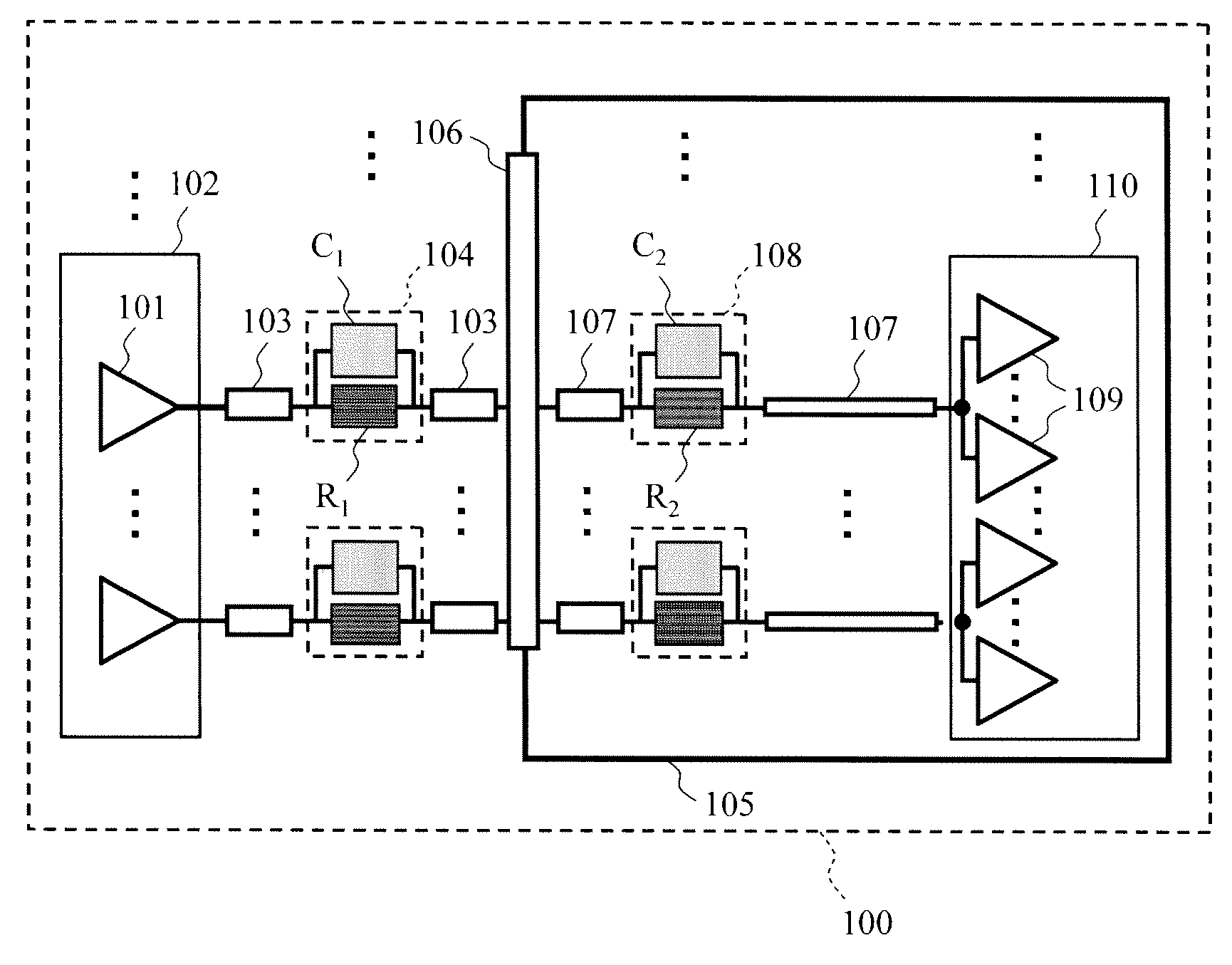
[0024]FIG. 1 is a configuration diagram of a data transmission system according to a first embodiment. The data transmission system is provided with a first Printed Circuit Board (PCB) 100 and a second Printed Circuit Board (PCB) 105, and both Printed Circuit Boards (PCB) can be connected and separated by a connector 106. The connector 106 is an example of a connection terminal for connecting the Printed Circuit Boards (PCB) so that the Printed Circuit Boards (PCB) can be electrically and mechanically connected and separated. A first semiconductor device 102 including at least one output buffer 101, a first trace 103 for transmitting data from the output buffer 101, first RC parallel circuits 104 including a re...


PUM


Abstract

A data transmission system is provided in which it is possible to perform both of suppressing the degrading of the slew rate and suppressing the ringing even if load capacitance of an input buffer is changed.
The data transmission system transmitting data from an output buffer to the input buffer through a trace is provided with first RC parallel circuits connected in series to the trace on a first Printed Circuit Board (PCB) on which the output buffer is mounted, and second RC parallel circuits connected in series to the trace on a second Printed Circuit Board (PCB) on which the input buffer is mounted, and which can be connected and separated to and from the first Printed Circuit Board (PCB).

Description

CLAIM OF PRIORITY[0001]The present application claims priority from Japanese patent application JP 2010-249998 filed on Nov. 8, 2010, the content of which is hereby incorporated by reference into this application.BACKGROUND OF THE INVENTION[0002]1. Field of the Invention[0003]The present invention relates to a data transmission system and a semiconductor circuit, and for example, relates to the data transmission system and the semiconductor circuit for transmitting data from an output buffer to an input buffer.[0004]2. Background Art[0005]There is an SSD (solid state drive) as a storage medium which is an alternative to a HDD (Hard disk drive). In recent years, to increase a storage capacity of the SSD, the number of memories trends to increase. When the number of memories increases, load capacitance of an input buffer increases, so that a slew rate of transmission data transmitted by an output buffer is degraded. To suppress the degrading of the slew rate, an internal series resist...

Claims


Application Information

Patent Timeline
Patent Type & Authority Applications(United States)
IPC IPC(8): H03H2/00H03H7/38
CPCH04B3/02
Inventor IKEDA, YASUHIROUEMATSU, YUTAKAMURAOKA, SATOSHI
Owner HITACHI LTD
Why Eureka
Try Eureka