

Nanosheet Device with Different Gate Lengths in Same Stack
a technology of nanosheet transistors and gate lengths, applied in the field of integrated nanosheet field effect transistors, can solve the problems of increasing the complexity of process integration used to define the features and structures of semiconductor devices, increasing the die area, and not being able to achieve the solution of fabricating nanosheet transistors
- Summary
- Abstract
- Description
- Claims
- Application Information
AI Technical Summary
Benefits of technology
Problems solved by technology
Method used
Image



Examples
Embodiment Construction
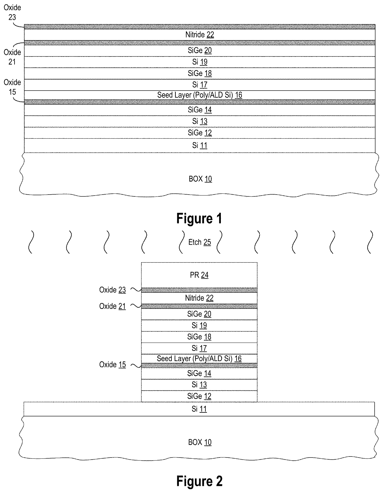
[0029]A semiconductor device and fabrication method are described for fabricating stacked nanosheet transistors with different gate lengths in the same stack in a single nanosheet process flow. While specific implementation details are described herein with reference to one or more example embodiments, the present disclosure is directed to an example processing sequence for fabricating nanosheet transistors in the same Si / SiGe stack with different gate lengths using additional process steps that are minimized to reduce complexity and cost. The process steps used for fabricating the stacked nanosheet transistors with different gate lengths are standard process steps, so no new fab tools may be needed. As an initial set of fabrication steps, a wafer substrate is formed with a stack of bottom and top Si / SiGe superlattice structures separated from one another by a barrier oxide layer, and then patterned and etched to form a transistor stack. With a first set of fabrication steps, the tr...
PUM
| Property | Measurement | Unit |
|---|---|---|
| thickness | aaaaa | aaaaa |
| thickness | aaaaa | aaaaa |
| gate length | aaaaa | aaaaa |
Abstract
Description
Claims
Application Information