
Application processor circuit incorporating both SD host and slave functions and electronic device including same
a technology of application processor and slave function, which is applied in the direction of coding, electric digital data processing, instruments, etc., can solve the problems of inability to enable data exchange between two pda devices and inability to achieve interconnection therebetween via such interfaces
- Summary
- Abstract
- Description
- Claims
- Application Information
AI Technical Summary
Benefits of technology
Problems solved by technology
Method used
Image

Examples
Embodiment Construction
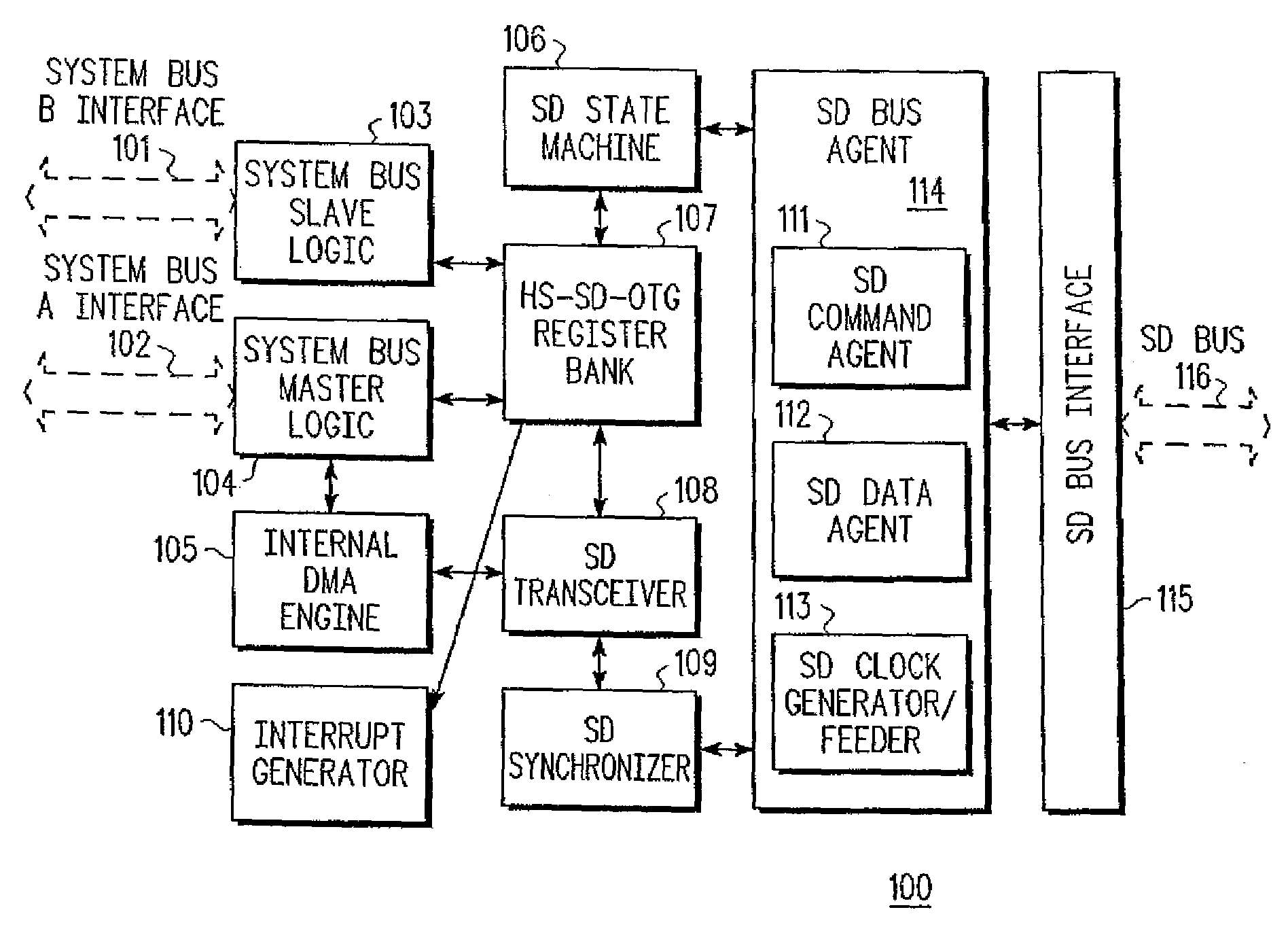
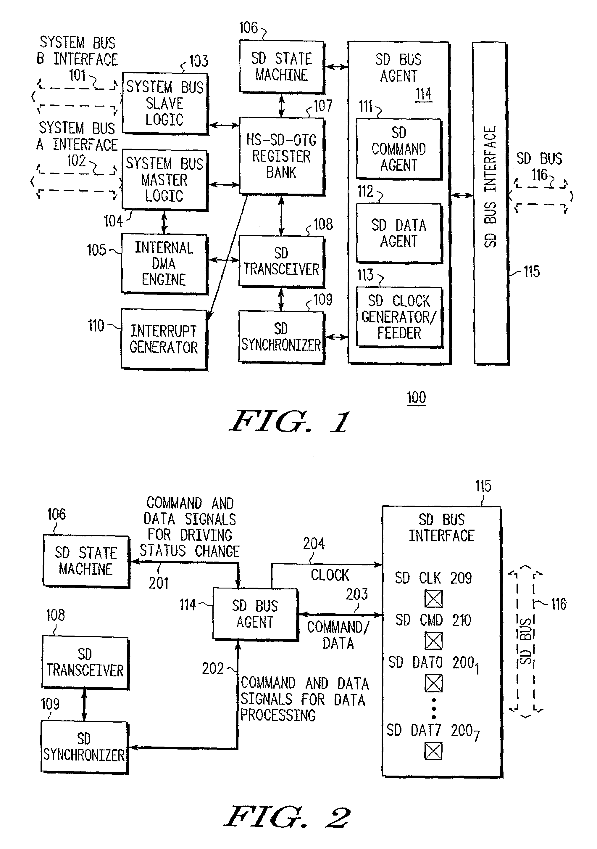
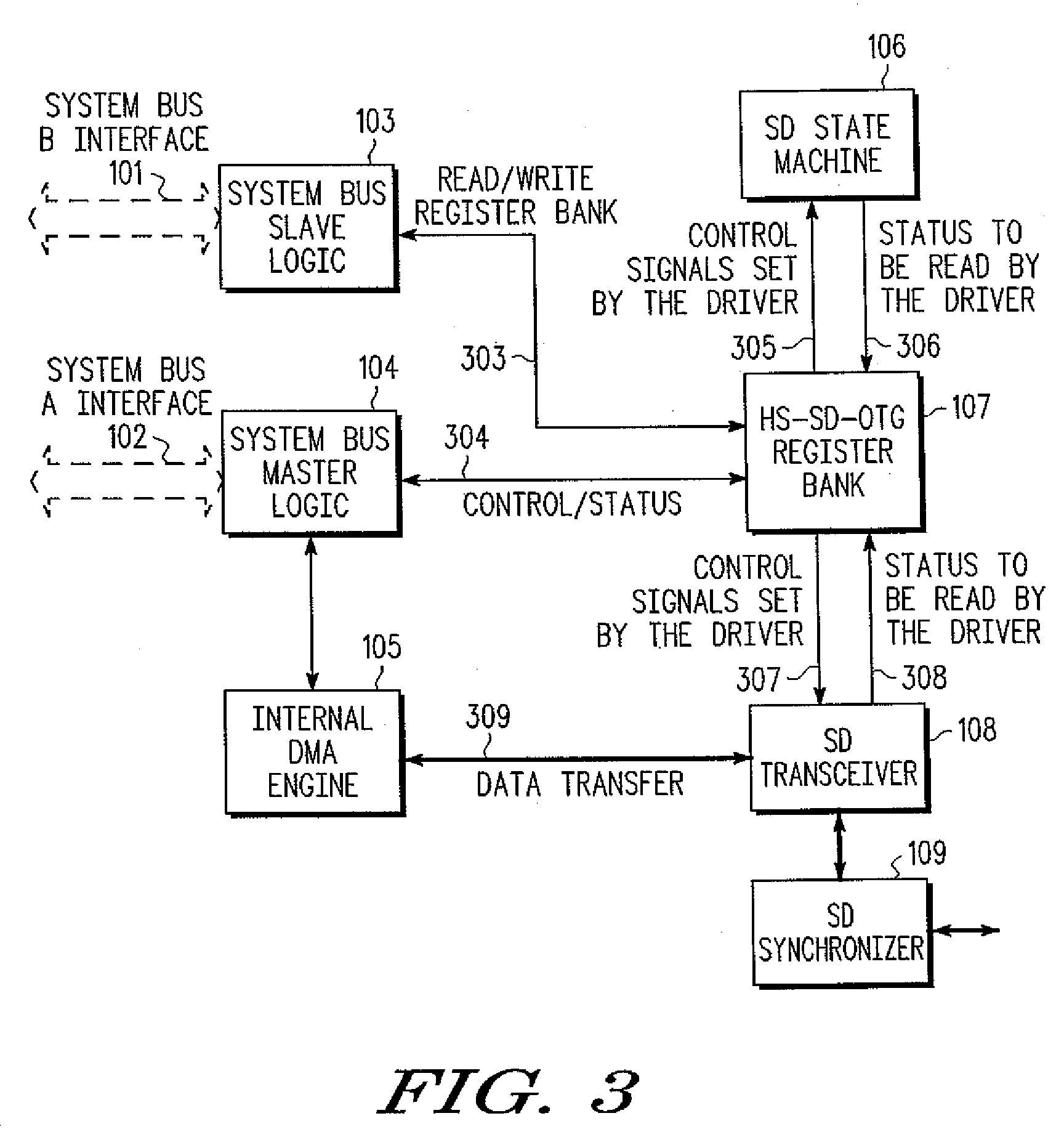
[0024]FIG. 1 illustrates generally the architecture of an application processor circuit 100 according to one embodiment of the present invention. The circuit 100 works in two bus domains, i.e., the system bus domain shown on the left side, and the SD bus domain shown on the right side of FIG. 1. In FIG. 1, system bus A interface 102 is used for data transfer. System bus A interface 102 is connected to system bus master logic 104. In FIG. 1, system bus B interface 101 is used for the configuration of a register bank (the configuration of the register bank is explained below). The system bus B interface 101 is connected to system bus slave logic 103. During data transfer by means of system bus A, system bus master logic 104 is used to select the devices on system bus A with which it conducts data transfer and is used to start data transfer. In one embodiment, separate system buses A and B are used respectively for configuration of functional modules and data transfer, to improve perfo...
PUM
 Abstract
Description
Claims
Application Information