
PLL circuit and semiconductor device
a technology of semiconductor devices and circuits, applied in the direction of pulse automatic control, oscillator generators, pulse techniques, etc., can solve the problems of capacitor capacitance and power consumption of pll circuits, and achieve the effects of preventing power consumption from becoming larg
- Summary
- Abstract
- Description
- Claims
- Application Information
AI Technical Summary
Benefits of technology
Problems solved by technology
Method used
Image

Examples
Embodiment Construction
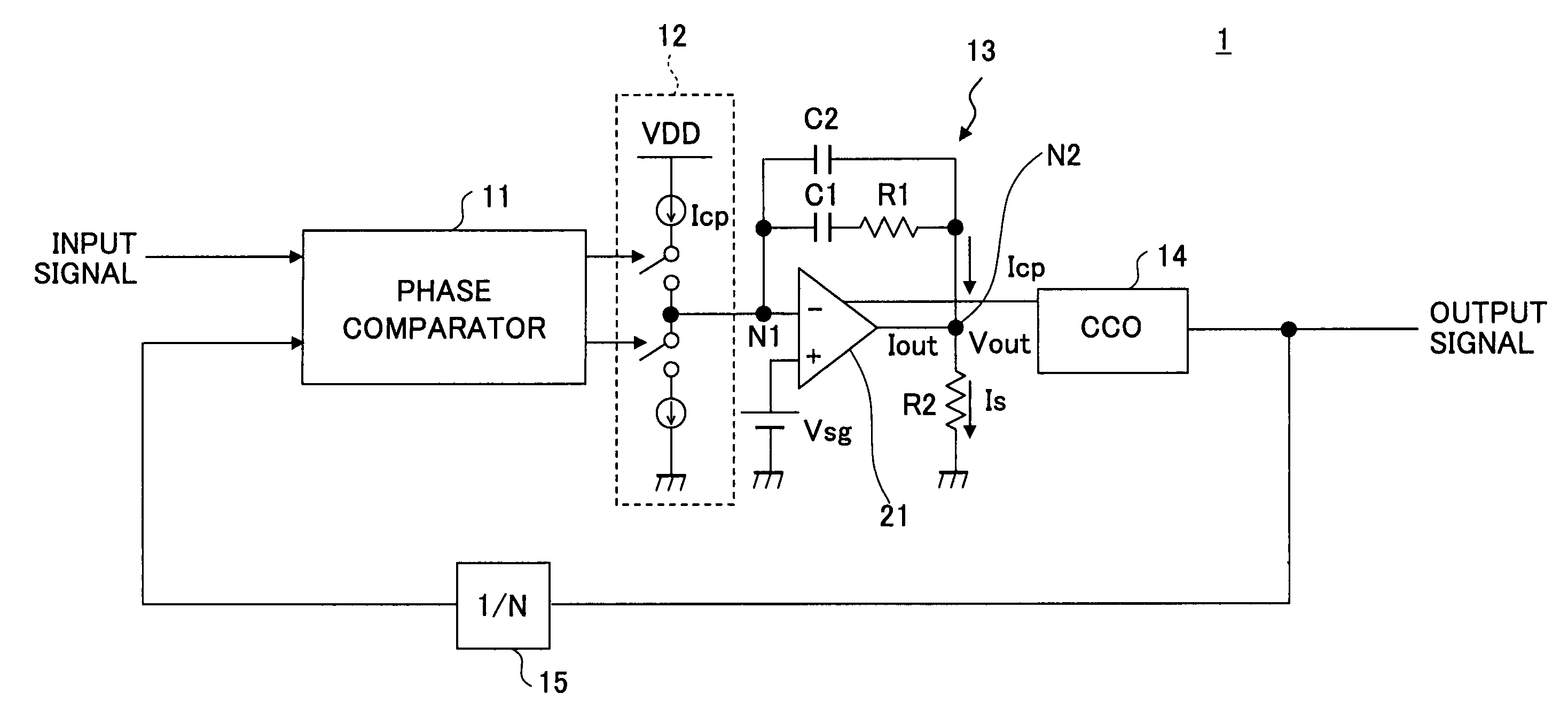
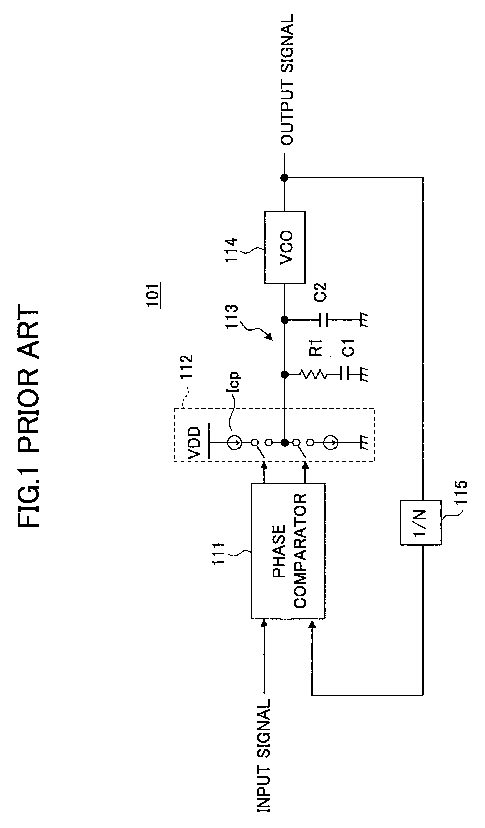
[0028]In the present invention, a LPF part including an amplifier, and a current controlled oscillator (CCO), are used in place of the PLL and the VCO that form the conventional PLL circuit. Hence, an apparent gain of the VCO, that is, the gain of the CCO, becomes smaller than the gain of the VCO of the conventional PLL circuit, and it is possible to prevent the power consumption from becoming large without interfering with the size reduction of the semiconductor integrated circuit.
[0029]A description will now be given of embodiments of the PLL circuit and the semiconductor device according to the present invention, by referring to FIG. 5 and the subsequent drawings.
[0030]FIG. 5 is a diagram showing an embodiment of the PLL circuit according to the present invention. A PLL circuit 1 has a phase comparator 11 that receives an input signal and a feedback signal which will be described later, a charge pump 12 that is controlled by an output of the phase comparator 11, a lowpass filter ...
PUM
 Abstract
Description
Claims
Application Information