PLL circuit and semiconductor device

a technology of semiconductor devices and circuits, applied in the direction of pulse automatic control, oscillator generators, pulse techniques, etc., can solve the problems of capacitor capacitance and power consumption of pll circuits, and achieve the effects of preventing power consumption from becoming larg

Inactive Publication Date: 2007-08-30
MONTEREY RES LLC
View PDF8 Cites 4 Cited by
  • Summary
  • Abstract
  • Description
  • Claims
  • Application Information

AI Technical Summary

Benefits of technology

[0011]Another and more specific object of the present invention is to provide a PLL circuit and a semiconductor device, which can prevent the power consumption from becoming large, without interfering with the size reduction of the semiconductor integrated circuit, even if the power supply voltage is relatively low.
[0012]Still another object of the present invention is to provide a phase locked loop circuit comprising a phase comparator configured to receive an input signal and a feedback signal; a charge pump controlled by an output of the phase comparator; a lowpass filter part configured to receive an output of the charge pump; a current controlled oscillator controlled by an output of the lowpass filter part; and a frequency divider configured to frequency-divide an output of the current controlled oscillator and to output the feedback signal, the lowpass filter part comprising an amplifier configured to receive the output of the charge pump and a reference voltage; and a circuit part, including capacitors and resistors, configured to receive the output of the charge pump and an output of the amplifier. According to the phase locked loop circuit of the present invention, it is possible prevent the power consumption from becoming large, without interfering with the size reduction of the semiconductor integrated circuit which includes the phase locked loop circuit, even if the power supply voltage is relatively low.
[0013]A further object of the present invention is to provide a semiconductor device comprising a phase locked loop circuit, the phase locked loop circuit comprising a phase comparator configured to receive an input signal and a feedback signal; a charge pump controlled by an output of the phase comparator; a lowpass filter part configured to receive an output of the charge pump; a current controlled oscillator controlled by an output of the lowpass filter part; and a frequency divider configured to frequency-divide an output of the current controlled oscillator and to output the feedback signal, the lowpass filter part comprising an amplifier configured to receive the output of the charge pump and a reference voltage; and a circuit part, including capacitors and resistors, configured to receive the output of the charge pump and an output of the amplifier. According to the semiconductor device of the present invention, it is possible to prevent the power consumption from becoming large, without interfering with the size reduction of the semiconductor integrated circuit which includes the phase locked loop circuit, even if the power supply voltage is relatively low.

Problems solved by technology

For this reason, there were problems in that the capacitance of the capacitor within the LPF increases by the amount corresponding to the increase of the gain of the VCO, and that the area occupied by the capacitor becomes large to thereby prevent the size reduction of the semiconductor integrated circuit.
Furthermore, there was a problem in that the power consumption of the PLL circuit becomes large due to the large gain of the VCO.

Method used


Image

  • PLL circuit and semiconductor device
  • PLL circuit and semiconductor device
  • PLL circuit and semiconductor device

Examples


Embodiment Construction

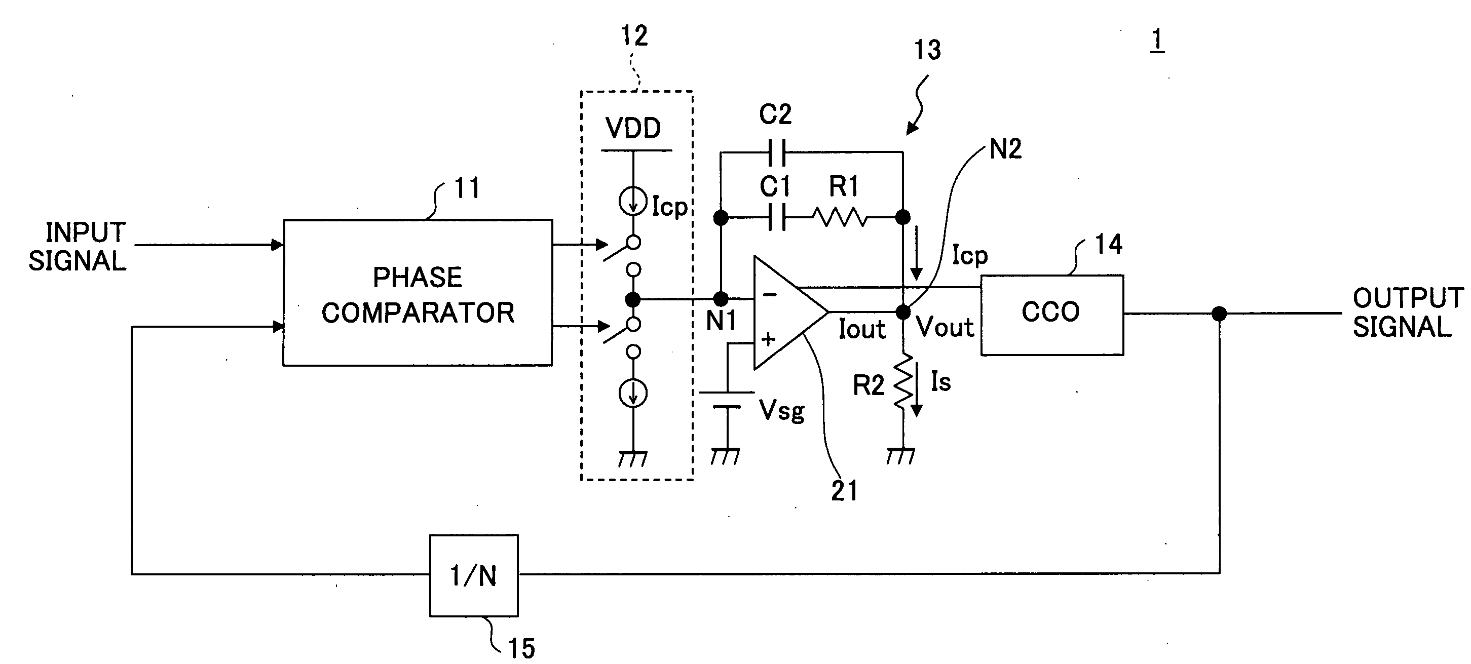
[0028]In the present invention, a LPF part including an amplifier, and a current controlled oscillator (CCO), are used in place of the PLL and the VCO that form the conventional PLL circuit. Hence, an apparent gain of the VCO, that is, the gain of the CCO, becomes smaller than the gain of the VCO of the conventional PLL circuit, and it is possible to prevent the power consumption from becoming large without interfering with the size reduction of the semiconductor integrated circuit.

[0029]A description will now be given of embodiments of the PLL circuit and the semiconductor device according to the present invention, by referring to FIG. 5 and the subsequent drawings.

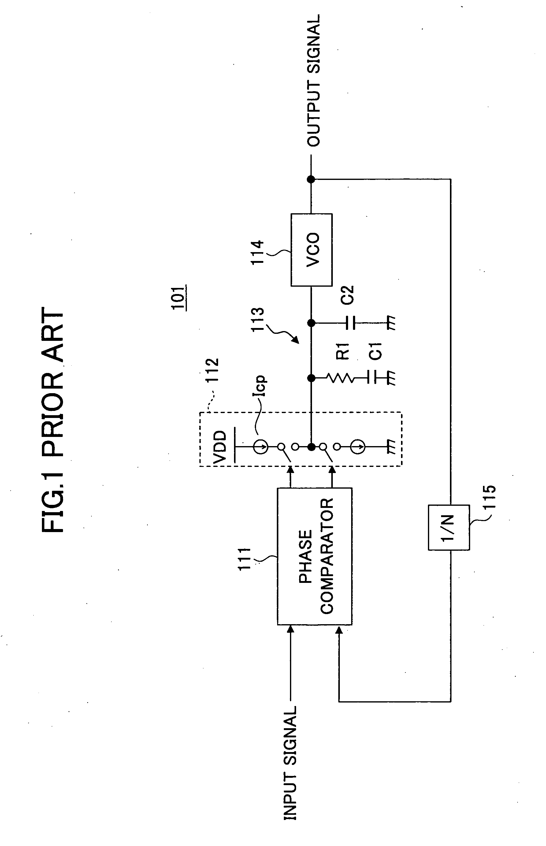
[0030]FIG. 5 is a diagram showing an embodiment of the PLL circuit according to the present invention. A PLL circuit 1 has a phase comparator 11 that receives an input signal and a feedback signal which will be described later, a charge pump 12 that is controlled by an output of the phase comparator 11, a lowpass filter ...


PUM


Abstract

A PLL circuit has a phase comparator to receive an input signal and a feedback signal, a charge pump controlled by an output of the phase comparator, a lowpass filter part to receive an output of the charge pump, a current controlled oscillator controlled by an output of the lowpass filter part, and a frequency divider to frequency-divide an output of the current controlled oscillator and to output the feedback signal. The lowpass filter part has an amplifier to receive the output of the charge pump and a reference voltage, and a circuit part including capacitors and resistors to receive the output of the charge pump and an output of the amplifier.

Description

BACKGROUND OF THE INVENTION[0001]1. Field of the Invention[0002]The present invention generally relates to phase locked loop (PLL) circuits and semiconductor devices, and more particularly to a PLL circuit that operates even at a relatively low power supply voltage and to a semiconductor device including such a PLL circuit.[0003]2. Description of the Related Art[0004]FIG. 1 is a diagram showing an example of a conventional PLL circuit. A PLL circuit 101 has a phase comparator 111 that receives an input signal and a feedback signal which will be described later, a charge pump 112 that is controlled by an output of the phase comparator 111, a lowpass filter (LPF) 113, a voltage controlled oscillator (VCO) 114, and a frequency divider 115. The LPF 113 is made up of a resistor R1 and capacitors C1 and C2. An output signal of the VCO 114 is subjected to a 1 / N frequency-division by the frequency divider 115, and is fed back to the phase comparator 111 as the feedback signal referred above...

Claims


Application Information

Patent Timeline
Patent Type & Authority Applications(United States)
IPC IPC(8): H03L7/00
CPCH03L7/1075H03L7/093
Inventor KODATO, KENICHIMATSUDA, ATSUSHI
Owner MONTEREY RES LLC
Why Eureka
Try Eureka