Active matrix display devices and portable electronic products using the same

a technology of active matrix and display device, which is applied in the direction of instruments, computing, electric digital data processing, etc., can solve the problems of increasing costs, more power consumption between source lines and gate lines, etc., and achieves the reduction of parasitic capacitance, slow battery capacity, and reduce power consumption.

Inactive Publication Date: 2009-11-19
INNOLUX CORP
View PDF3 Cites 35 Cited by
  • Summary
  • Abstract
  • Description
  • Claims
  • Application Information

AI Technical Summary

Benefits of technology

[0016]The active matrix display device of the invention may be applied in a portable electronic product such as a mobile phone, a PDA, a walkman, or a portable game console etc. The portable electronic product is typically driven with batteries. Consequently, using the active matrix display device of the invention to restrain power consumption makes the capacity of the batteries decrease slower than before.
[0017]Thus, an active matrix display device having a plurality of pixels arranged in rows and columns, and portable electronic products using the same is provided, wherein parasitic capacitance is decreased and requirement for an additional driving device is eliminated.

Problems solved by technology

However, parasitic capacitance causing more power consumption exists between the source lines and the gate lines.
The problem is especially prevalent, when the active matrix display device is applied in portable battery-driven devices such as mobile phones.
However, an additional driving device is required, thus increasing costs.

Method used


Image

  • Active matrix display devices and portable electronic products using the same
  • Active matrix display devices and portable electronic products using the same
  • Active matrix display devices and portable electronic products using the same

Examples


first embodiment

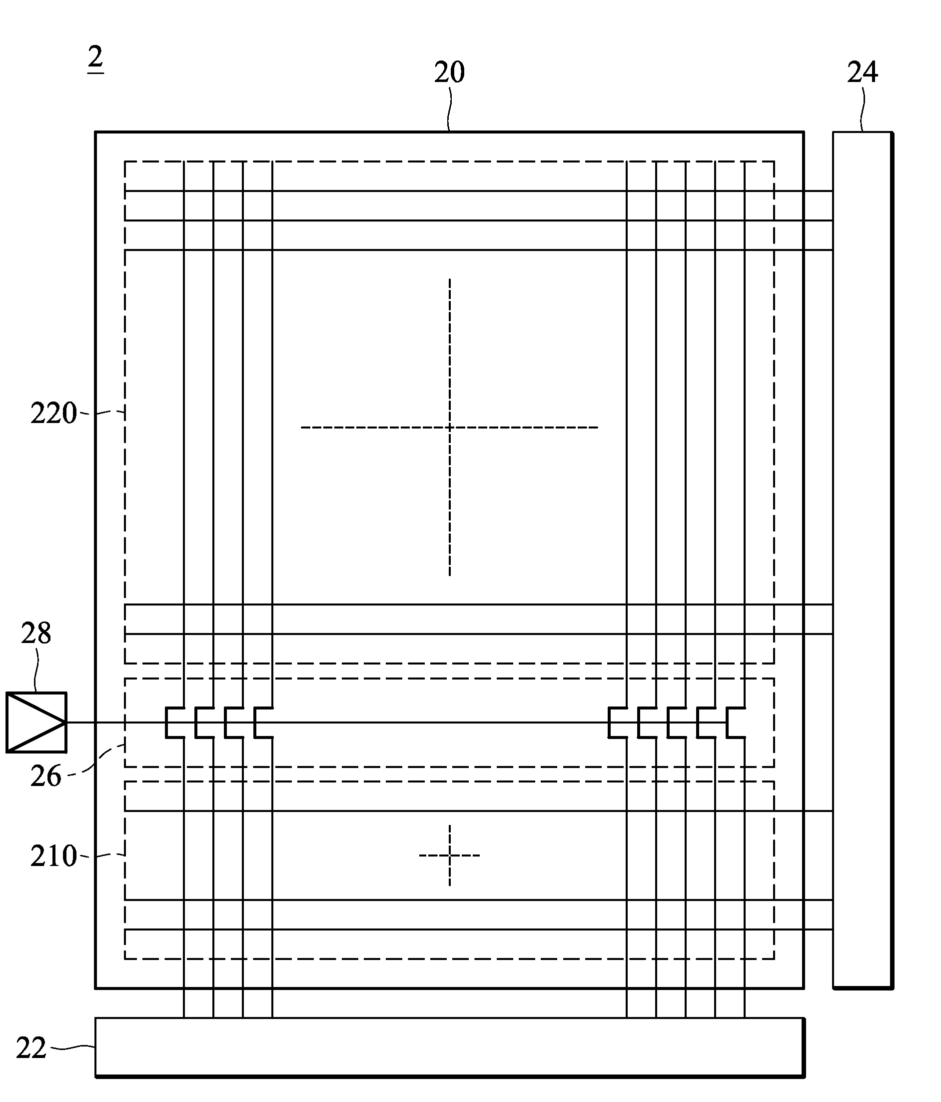
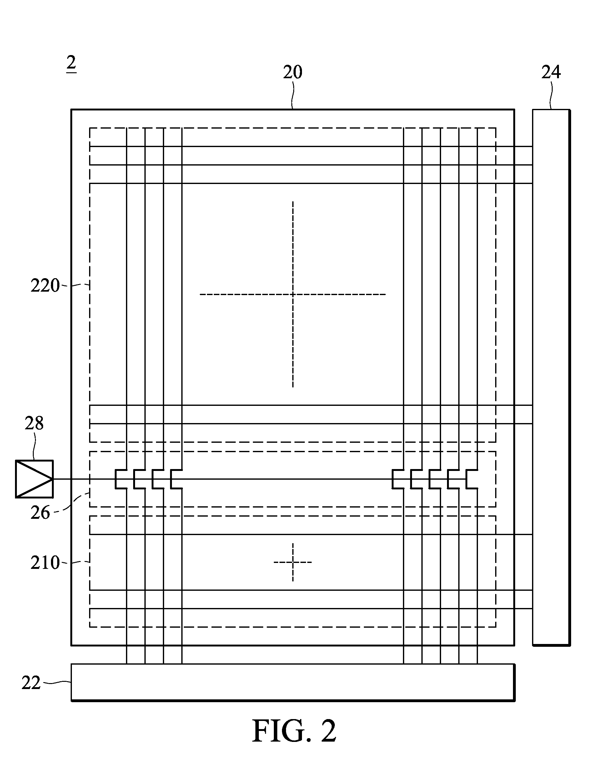
[0031]FIG. 2 shows an active matrix display device of the present invention. A display device 2 in FIG. 2 includes a display area 20, having a plurality of pixels arranged in rows and columns; a source driving device 22, providing power or electric charges for the pixels through source lines; a gate driving device 24, controlling on / off of the pixels through gate lines; a boundary switch 26, separating the display area 20 into a first sub-display area 210 and a second sub-display area 220 and placed therebetween to connect or disconnect the source lines; and a switch driving device 28. The first sub-display area and second sub-display area are disposed at the upper and lower side of the boundary switch 26, respectively. Each pixel has at least one driving transistor and at least one display element (ex. a liquid crystal cell, or an organic light-emitting diode, etc). Every pixel in the same row shares a gate line connecting to its driving transistor. Every pixel in the same column s...

second embodiment

[0035]FIG. 4 shows an active matrix display device of the present invention. A display device 4 in FIG. 4 includes a display area 40, having a plurality of pixels arranged in rows and columns; a source driving device 42, providing power or electric charges for the pixels through source lines; a gate driving device 44, controlling on / off of the pixels through gate lines; a boundary switch 46, separating the display area 40 into a first sub-display area 410 and a second sub-display area 420 and placed therebetween to connect or disconnect the gate lines; and a switch driving device 48, controlling on / off of the boundary switch 46. The first sub-display area and second sub-display area are disposed at the left and right side of the boundary switch 46, respectively. Each pixel has at least one driving transistor and at least one display element (ex. a liquid crystal cell, or an organic light-emitting diode, etc). Every pixel in the same row shares a gate line connecting to its driving t...

third embodiment

[0040]FIG. 5 shows an active matrix display device of the present invention. A display device 5 in the FIG. 5 includes a display area 50, having a plurality of pixels arranged in rows and columns; source driving devices 52, 53, providing power or electric charges for the pixels through source lines; gate driving devices 54, 55, controlling on / off of the pixels through gate lines; a boundary switch 56, separating the display area 50 into a first sub-display area 510 and a second sub-display area 520 and placed therebetween to connect or disconnect the source lines; and a switch driving device 58, controlling on / off of the boundary switch 56. Each pixel has at least one driving transistor and at least one display element (ex. a liquid crystal cell, an organic light-emitting diode, etc). Every pixel in the same row shares a gate line connecting to its driving transistor. Every pixel in the same column shares a source line supplying power or electric charges thereto.

[0041]The display de...


PUM


Abstract

The display device of the present invention includes a display area having a plurality of pixels arranged in rows and columns, at least one source driving device providing power or electric charges for the pixels through source lines, at least one gate driving device controlling the pixels through gate lines, and a boundary switch separating the display area into a plurality of sub-display areas and placed between the sub-display areas to connect or disconnect the source lines and/or the gate lines. When the boundary switch disconnects the source lines and/or the gate lines, the sub-display area directly connecting with the source driving device or the gate driving device will be driven.

Description

CROSS REFERENCE TO RELATED APPLICATIONS[0001]This application claims the benefit of J.P. Patent Application No. 2008-127453, filed May, 14, 2008.FIELD OF THE INVENTION [0002]The present invention relates to active matrix display devices and portable electronic products using the same, and more particularly to active matrix display devices having a plurality of pixels arranged in rows and columns, and portable electronic products using the same.DESCRIPTION OF THE PRIOR ART [0003]An active matrix display device includes a display area having a plurality of pixels arranged in rows and columns. Each pixel has at least one driving transistor and display element (ex. a liquid crystal cell or an organic light-emitting diode), and so on. Every pixel in the same row shares a gate line connecting to a driving transistor thereof. A gate driving device transmits control signals to the pixels through the gate lines to control on / off of the pixels. Every pixel in the same column shares a source l...

Claims


Application Information

Patent Timeline
Patent Type & Authority Applications(United States)
IPC IPC(8): G06F3/038
CPCG02F1/1345G02F1/136286G09G3/3225G09G3/3266G09G3/3275G09G2330/021G09G3/3677G09G3/3688G09G2300/0857G09G2310/0221G09G2310/0297G09G3/3666
Inventor YAMASHITA, KEITARO
Owner INNOLUX CORP
Why Eureka
Try Eureka