Switch-body PMOS switch with switch-body dummies

a switch body and switch technology, applied in the field of switch body pmos switch, can solve the problems of imposing methods, reducing the efficiency of actual operating s/h devices, and affecting the efficiency of actual operation, so as to reduce the non-linearity error

Inactive Publication Date: 2011-06-28
NXP BV
View PDF6 Cites 8 Cited by
  • Summary
  • Abstract
  • Description
  • Claims
  • Application Information

AI Technical Summary

Benefits of technology

Among other features and benefits, this one aspect of one example second and fourth embodiments, namely applying a gate control and a body bias to the PMOS dummy FETs opposite to the gate control and the

Problems solved by technology

It has been long known, however, to persons of ordinary skill in the arts pertaining to S/H devices that actual operating S/H devices suffer from various non-ideal characteristics by which the actual sample at a given time after the sampling instant is not, in fact, the exact value of the input signal that was extant at that instant.
An inherent problem faced by a single transistor PMOS FET or NMOS FET structure is that each requires a threshold gate-to-source voltage, generally termed VTH, to switch on, meaning to form a conducting channel extending under the gate from the source to the drain.
This method imposes costs, and has ot

Method used


Image

  • Switch-body PMOS switch with switch-body dummies
  • Switch-body PMOS switch with switch-body dummies
  • Switch-body PMOS switch with switch-body dummies

Examples


Embodiment Construction

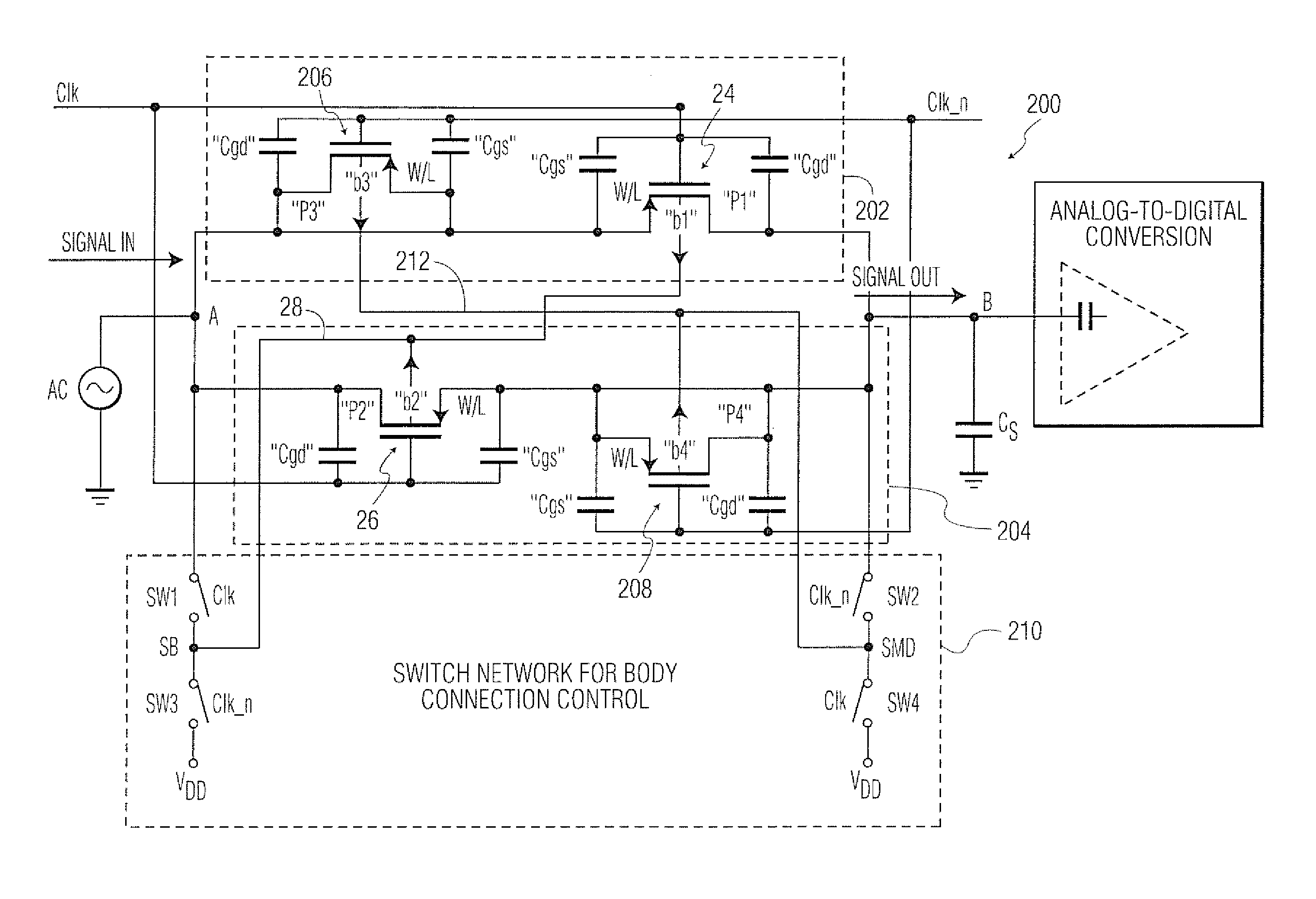
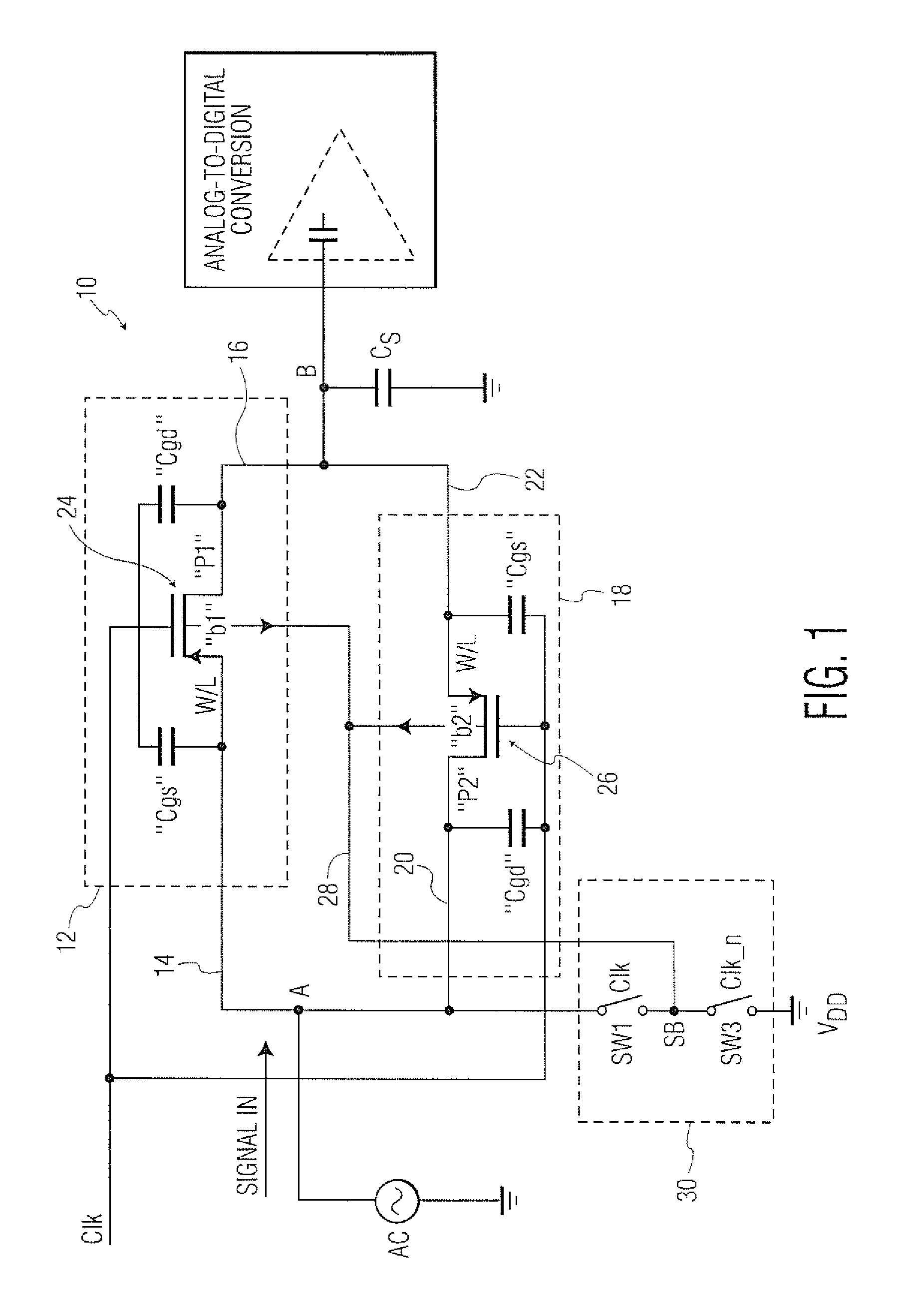
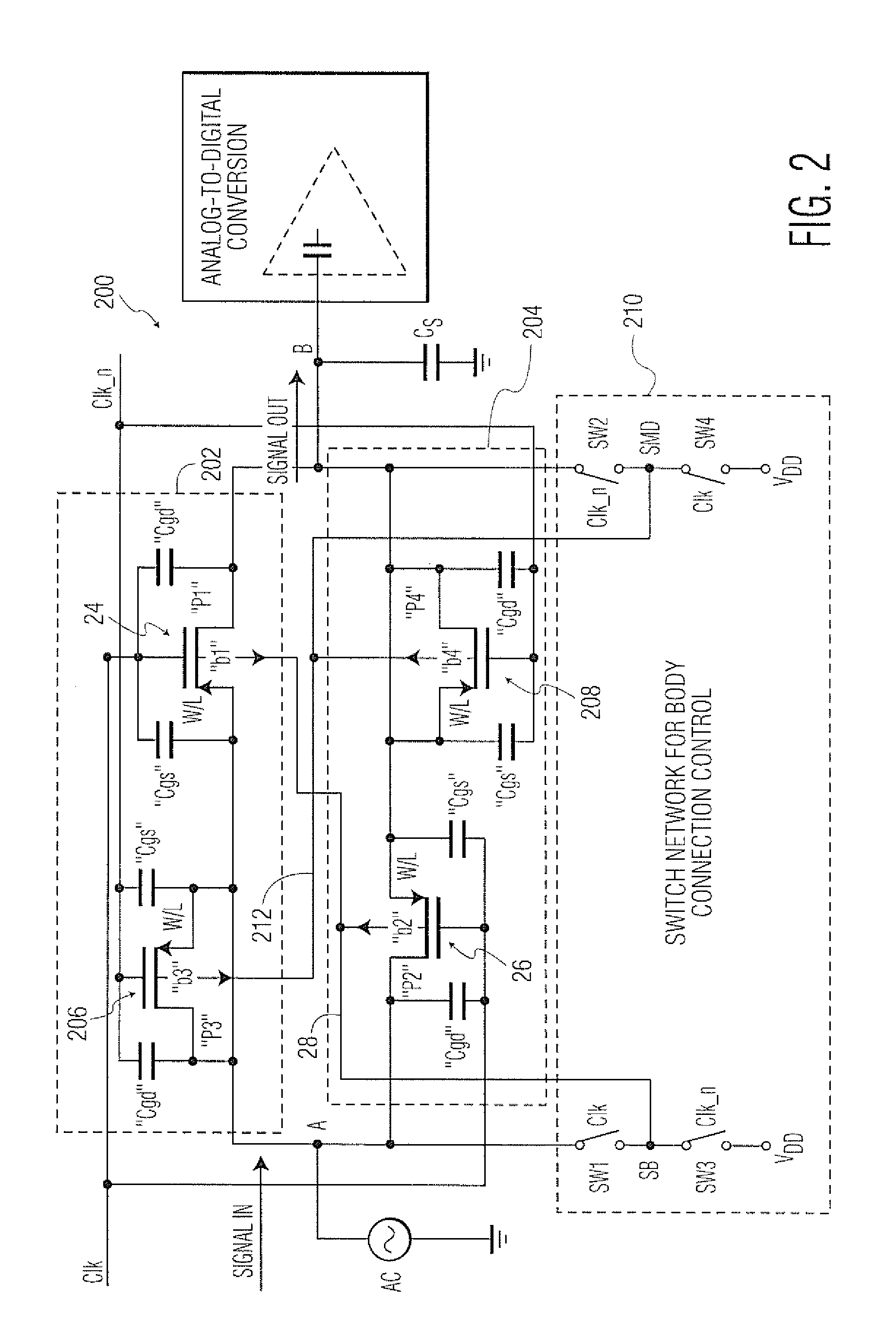
Various examples having one or more exemplary embodiments are described in reference to specific example configurations and arrangements. The specific examples are only for illustrative purposes, selected to further assist a person of ordinary skill in the art of sample-and-hold circuits to form an understanding of the concepts sufficient for such a person, applying the knowledge and skills such person possesses, to practice the invention. Neither the scope of the embodiments and the range of implementations, however, are limited to these specific illustrative examples. On the contrary, as will be recognized by persons of ordinary skill in the sample-and-hold arts upon reading this description, other configurations, arrangements and implementations practicing one or more of the embodiments, and one or more various aspects of each, may be designed and constructed.

The figures are arranged to provide a clear depiction of the figure's illustrated example subject matter and, further, gra...


PUM


Abstract

An analog sample-and-hold switch has parallel branches extending from an input node to an output node connected to a hold capacitor, each branch having a PMOS signal switch FET in series with a PMOS dummy FET. A sample clock controls on-off switching of the PMOS signal switch FETs, and an inverse of the sample clock controls a complementary on-off switching of the PMOS dummy FETs. A bias sequencer circuit biases the PMOS signal switch FETs and biases the PMOS dummy FETs, in a complementary manner, synchronous with their respective on-off states. The on-off switching of the PMOS dummy FETs injects charge cancelling a charge injection by the PMOS signal switch FETs, and injects glitches cancelling glitches injected by the PMOS signal switch FETs.

Description

TECHNICAL FIELDThe technical field relates generally to circuits for sampling and holding an instantaneous value of a time-varying electrical signal.BACKGROUNDA sample-and-hold circuit receives an electrical signal with one or more time varying attributes such as, for example, amplitude or phase and, in response to a sampling command event such as, for example, a clock edge, takes and holds a sample of the signal.Sample and hold devices (hereinafter referenced generically as “S / H device(s)”), are used in a wide range of applications such as, for example, a pre-sampler within, or preceding a front end of an analog-to-digital converter (“ADC”), typically to present a value to the comparators of the ADC that is reasonably stationary for long enough to meet a set-up and hold time requirement of the ADC, or a “de-glitches” installed at the output of a digital-to-analog converter (“DAC”), typically to sample the DAC output at some time after the DAC clock and thus hold a steady-state anal...

Claims


Application Information

Patent Timeline
IPC IPC(8): G11C27/02
CPCH03K17/164
Inventor WU, QIONGMAHOOTI, KEVIN
Owner NXP BV
Why Eureka
Try Eureka