
Delay circuit
a delay circuit and circuit technology, applied in the field of delay circuits, can solve the problems of difficulty in making the delay time more accurate, easy variation of the impedance component, and difficulty in ensuring the accuracy of the delay tim
- Summary
- Abstract
- Description
- Claims
- Application Information
AI Technical Summary
Benefits of technology
Problems solved by technology
Method used
Image

Examples
Embodiment Construction
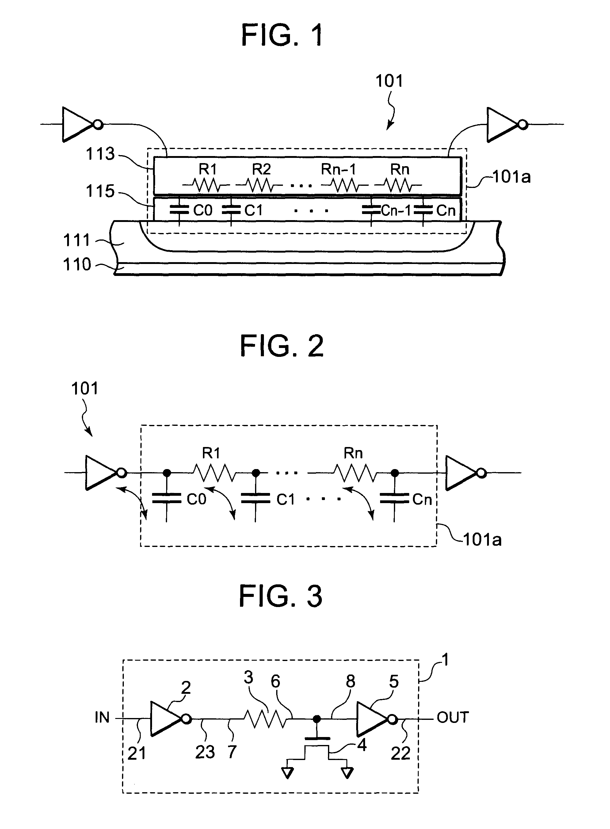
[0021]Hereinafter, a delay circuit according to an embodiment of the present invention will be described with reference to the attached drawings. FIG. 3 is a circuit diagram showing the configuration of the delay circuit according to the embodiment of the present invention. A delay circuit 1 includes an inverter 2, a resistance element 3, a capacitor element 4 and an inverter 5.
[0022]The inverter 2 has an input side connected to a wiring 21 which is a supply source of a signal, and has an output side connected to a wiring 23 which is an output destination of the signal. The wirings 21 and 23 are exemplified by metal wirings. The resistance element 3 has one end connected to the wiring 23, and the other end connected to a wiring 6. The resistance element 3 is exemplified by a polysilicon layer. The wiring 6 is exemplified by a silicide layer (+ a polysilicon layer). The capacitor element 4 has one end connected to the wirings 6 and 8, and the other end buried in a semiconductor subst...
PUM
 Abstract
Description
Claims
Application Information