

Thin film transistor array panel and method of manufacturing the same
a technology of thin film transistors and array panels, which is applied in the field of thin film transistor array panels, can solve the problems of delay of gate voltage applied through the gate line of a conventional structure, the size of lcds is increasing, and the inability to remove color filters or light blocking components, etc., to achieve the effect of improving resolution, reducing delay of signal, and increasing the thickness of gate lines
- Summary
- Abstract
- Description
- Claims
- Application Information
AI Technical Summary
Benefits of technology
Problems solved by technology
Method used
Image

Examples
Embodiment Construction
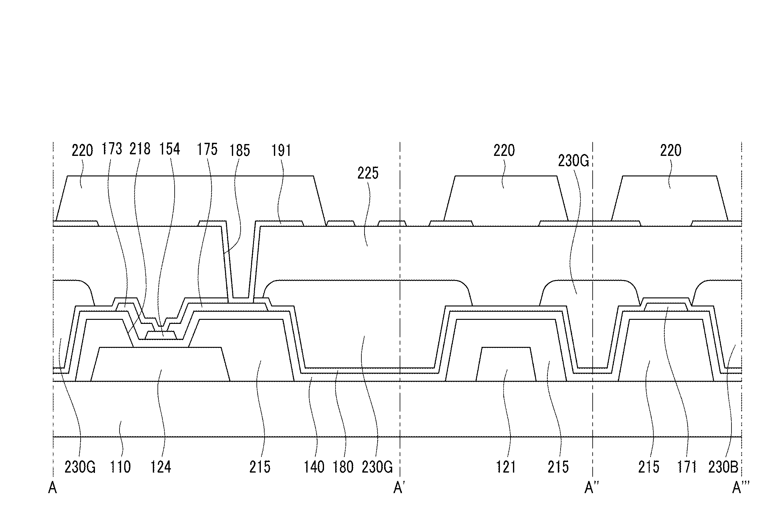
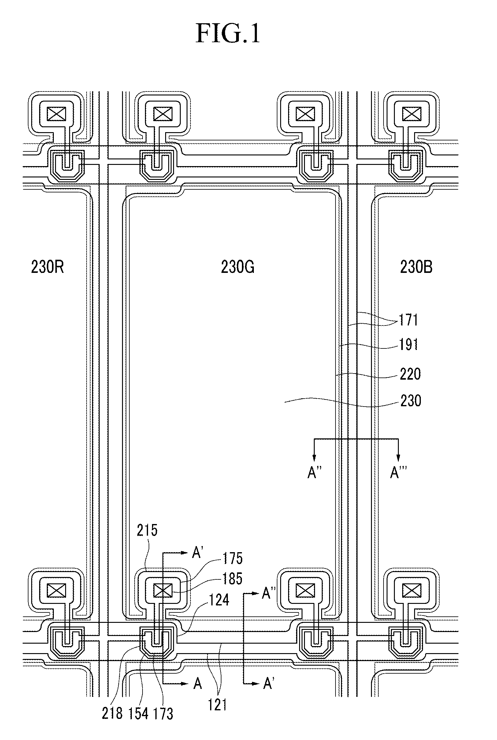
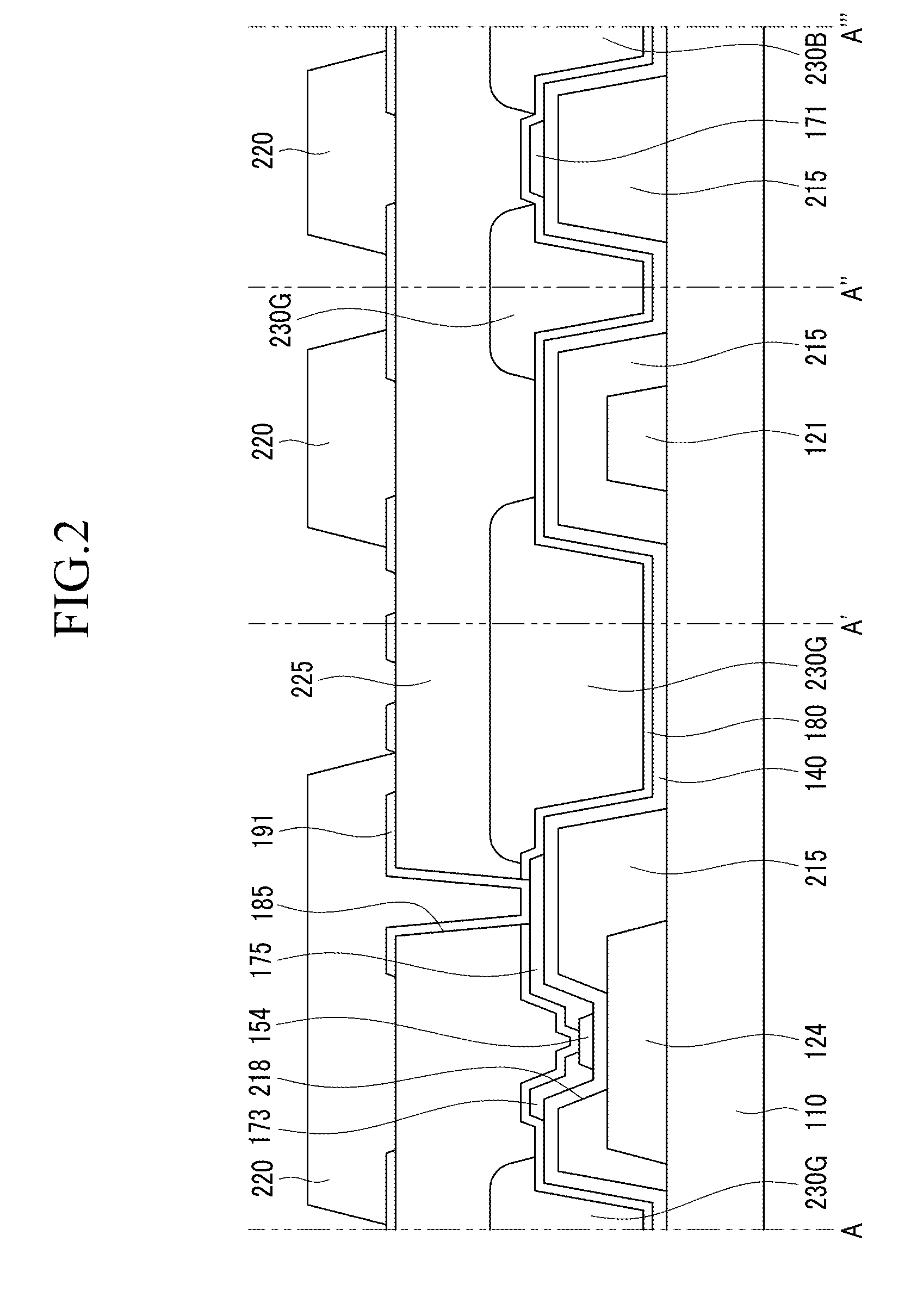
[0059]The present invention will be described more fully hereinafter with reference to the accompanying drawings, in which exemplary embodiments of the invention are shown. As those skilled in the art would realize, the described embodiments may be modified in various different ways, all without departing from the spirit or scope of the present invention.
[0060]In the drawings, the thickness of layers, films, panels, regions, etc., are exaggerated for clarity. Like reference numerals designate like elements throughout the specification. It will be understood that when an element such as a layer, film, region, or substrate is referred to as being “on” another element, it can be directly on the other element or intervening elements may also be present. In contrast, when an element is referred to as being “directly on” another element, there are no intervening elements present.
[0061]It will be understood that, although the terms first, second, third etc. may be used herein to describe v...
PUM
| Property | Measurement | Unit |
|---|---|---|
| dielectric constant | aaaaa | aaaaa |
| thickness | aaaaa | aaaaa |
| thickness | aaaaa | aaaaa |
Abstract
Description
Claims
Application Information