Display apparatus

a display device and display technology, applied in the field of display devices, can solve problems such as unfavorable degradation of image quality, and achieve the effect of improving display quality

Inactive Publication Date: 2013-01-29
SHARP KK
View PDF11 Cites 1 Cited by
  • Summary
  • Abstract
  • Description
  • Claims
  • Application Information

AI Technical Summary

Benefits of technology

[0054]As described above, a display device according to the present invention is a display device of an active-matrix type having a plurality of pixels arranged in rows and columns, including: scanning signal lines; a scanning signal line driving circuit that drives the scanning signal lines; auxiliary capacitor signal lines formed in each separate one of the rows; and an auxiliary capacitor signal line driving circuit that drives the auxiliary capacitor signal lines, the scanning signal line driving circuit supplying scanning signals, the auxiliary capacitor signal line driving circuit supplying auxiliary capacitor signals, the scanning signals and the auxiliary capacitor signals being supplied to a display region through one and the same edge of or opposite and different edges of the display region, each of the rows being provided with a plurality of the scanning signal lines for supplying those ones of the scanning signals which have different pulse widths from each other, the pixels of the same row being divided into a plurality of groups according to which of the scanning signal lines the pixels are connected to, the plurality of groups being arranged along the scanning signal lines, the pulse widths of the scanning signals that are supplied to the respective groups being set according to a position of each of the groups with respect to the auxiliary capacitor signal line driving circuit such that that one of the groups which is further from a point close to one edge near the auxiliary capacitor signal line driving circuit with respect to the auxiliary capacitor signal line driving circuit is supplied with that one of the scanning signals which has a smaller pulse width.
[0055]The foregoing configuration makes it possible not only to prevent a horizontal shadow in the display device, but also to control to a desired level the effective value of a voltage that is applied to each display element, thus bringing about an effect of making it possible to improve display quality by controlling the luminance of each display element to a desired level.

Problems solved by technology

However, an attempt to achieve an active-matrix liquid crystal display device or, in particular, an active-matrix liquid crystal display device having a wider display screen with higher resolution makes shadows likely to appear, thus undesirably degrading image quality.

Method used


Image

  • Display apparatus
  • Display apparatus
  • Display apparatus

Examples


embodiment 1

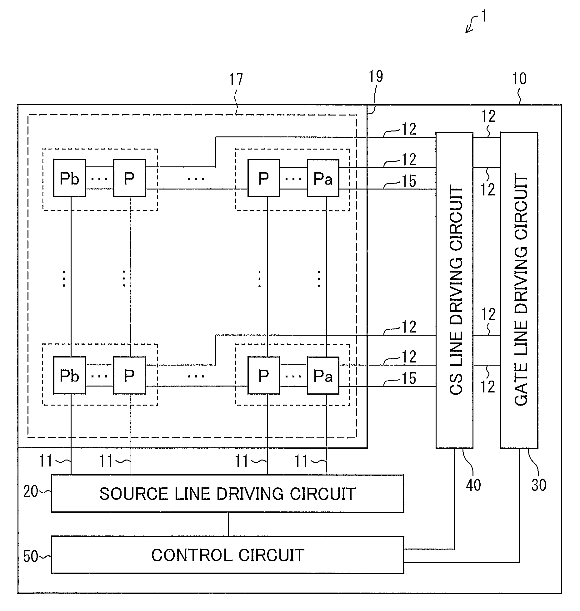
[0071]First, a configuration of a liquid crystal display device (display device) in accordance with the present embodiment is described with reference to FIGS. 1 through 3. FIG. 1 is a block diagram showing an overall structure of a liquid crystal display device.

[0072]As shown in FIG. 1, a liquid crystal display device 1 includes an active-matrix liquid crystal display panel 10, a source line driving circuit (data signal line driving circuit) 20, a gate line driving circuit (scanning signal line driving circuit) 30, a CS line driving circuit (auxiliary capacitor signal line driving circuit) 40, and a control circuit 50.

[0073]The liquid crystal panel 10 includes: an active-matrix substrate (not illustrated), a counter substrate (not illustrated), liquid crystals sandwiched between the active-matrix substrate and the counter substrate; and a plurality of pixels P (including Pa and Pb) arranged in rows and column.

[0074]Moreover, the liquid crystal display panel 10 includes source lines...

embodiment 2

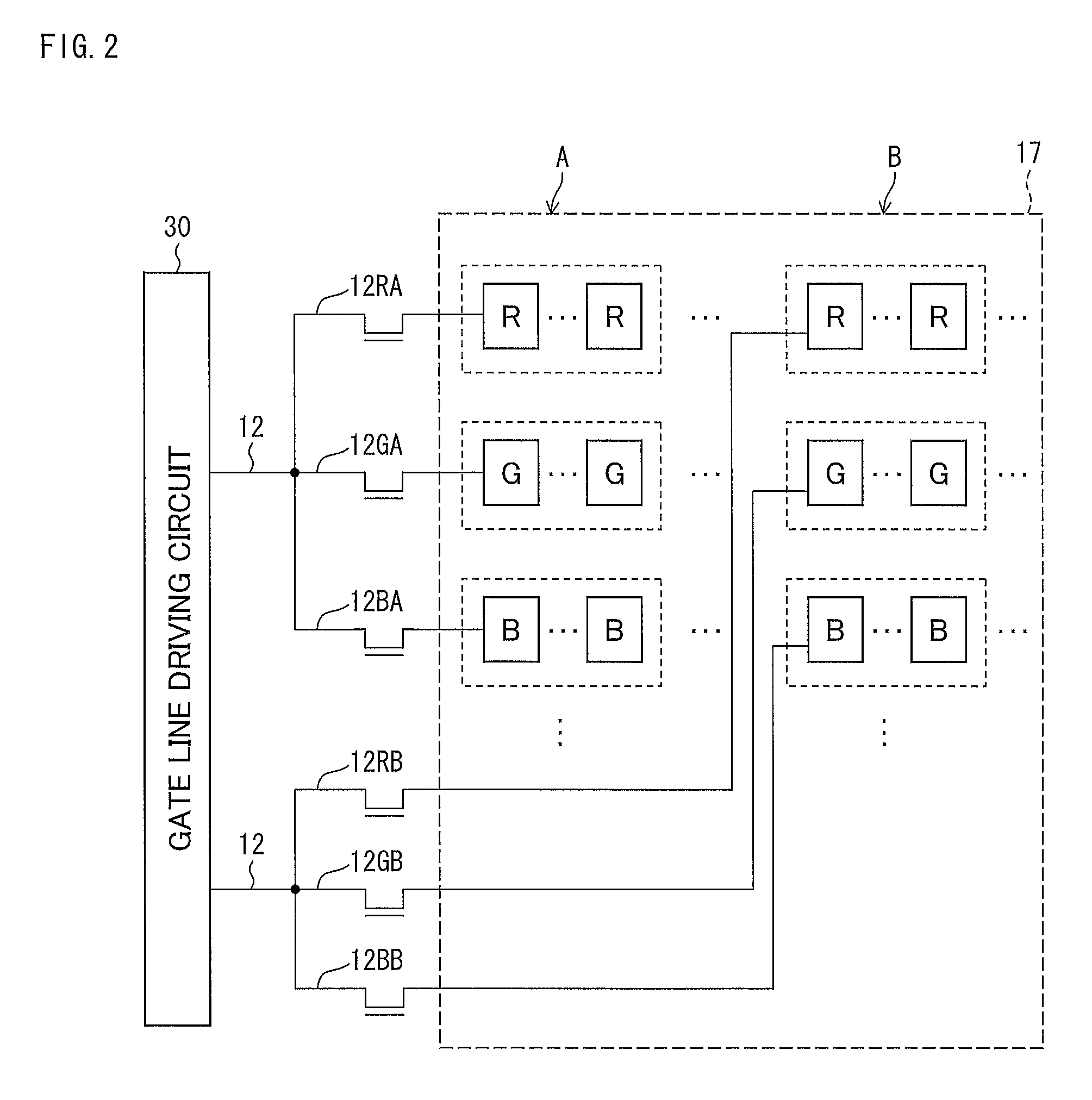
[0109]Another embodiment of a liquid crystal display device (display device) of the present invention described below with reference to FIG. 8.

[0110]For convenience of explanation, those members which have the same functions as those shown in the drawings described above in Embodiment 1 are given the same reference signs, and as such, are not described below.

[0111]FIG. 8 is a block diagram showing an overall structure of a liquid crystal display device in accordance with the present embodiment.

[0112]As shown in FIG. 8, a liquid crystal display device 2 has CS line driving circuits (auxiliary capacitor signal line driving circuits) 40 and gate line driving circuits (scanning signal line driving circuits) 30 each disposed on either side of a liquid crystal panel 10, and gate signals that are supplied by the gate line driving circuit 30 and CS signals that are supplied by the CS line driving circuit 40 are supplied to a display region 17 through one edge of the display region 17 and an...

embodiment 3

[0120]Another embodiment of a liquid crystal display device (display device) of the present invention described below with reference to FIG. 9.

[0121]For convenience of explanation, those members which have the same functions as those shown in the drawings described above in Embodiment 1 are given the same reference signs, and as such, are not described below.

[0122]FIG. 9 is a block diagram showing a configuration of a liquid crystal display device in accordance with the present embodiment.

[0123]As shown in FIG. 9, a liquid crystal display device 3 is configured such that each of the rows is provided with a plurality of CS signal lines 15 for supplying CS signals having different potentials from each other, that the pixels P of the same row are divided into a plurality of groups according to which of the CS signal lines 15 the pixels P are connected to, the plurality of groups being arranged along the gate lines 12, and that the potentials of the CS signals that are supplied to the r...


PUM

PropertyMeasurementUnit
pulse widthsaaaaaaaaaa
widthaaaaaaaaaa
pulse widthaaaaaaaaaa

Abstract

A liquid crystal display panel (10) includes: an active-matrix substrate (not illustrated), a counter substrate (not illustrated), liquid crystals sandwiched between the active-matrix substrate and the counter substrate; and a plurality of pixels (P) arranged in rows and columns. Each of the rows is provided with a plurality of gate signal lines (12) for supplying scanning signals having different pulse widths from each other, and the pixels of the same row are divided into a plurality of groups according to which of the gate signal lines (12) the pixels are connected to. The pulse widths of the scanning signals that are supplied to the respective groups are set according to the position of each of the groups with respect to an auxiliary capacitor signal line driving circuit (40) such that one of the groups which is further from a point close to one edge near the auxiliary capacitor signal line driving circuit (40) with respect to the auxiliary capacitor signal line driving circuit (40) is supplied with that one of the scanning signals which has a smaller pulse width.

Description

TECHNICAL FIELD[0001]The present invention relates to display devices and, in particular, to an active-matrix display device.BACKGROUND ART[0002]In recent years, there has been a rapidly growing demand for liquid crystal display devices, etc. in the form of flat panel displays. Since liquid crystal display devices consume less electric power and can be more easily made in a small size than CRTs (cathode-ray tubes), liquid crystal display devices have been widely used in cellular phones, portable game machines, in-vehicle navigation systems, etc., as well as televisions. Among these liquid crystal display devices, active-matrix liquid crystal display devices have been widely used because they are high in response speed and make it easy to display multiple tones.[0003]However, an attempt to achieve an active-matrix liquid crystal display device or, in particular, an active-matrix liquid crystal display device having a wider display screen with higher resolution makes shadows likely to...

Claims


Application Information

Patent Timeline
Patent Type & Authority Patents(United States)
IPC IPC(8): G02F1/1343
CPCG09G3/3677G09G2300/0426G09G2310/0218G09G2310/0281G09G2310/08G09G2320/0209G09G2320/0223
Inventor YOKOYAMA, YOHSUKE
Owner SHARP KK
Why Eureka
Try Eureka