Low power comparator with fast propagation delay

a low-power comparator and propagation delay technology, applied in the field of integrated circuit comparators, can solve the problems of power supply rejection and longer propagation delay, and achieve the effect of quick response to applied voltages

Active Publication Date: 2009-07-14
NAT SEMICON CORP
View PDF14 Cites 1 Cited by
  • Summary
  • Abstract
  • Description
  • Claims
  • Application Information

AI Technical Summary

Benefits of technology

[0006]To address the above-discussed deficiencies of the prior art, it is a primary object of the present invention to provide, for use in an integrated circuit comparator, a pulsed rather than continuous bias current applied, in at least a fast comparator configuration, to a current source within a comparator's input gain stage. The transconductance current will then be pulsed rather than continuous. The pulse width of the bias current is small relative to the system clock, but has a large current magnitude allowing the comparator to quickly respond to applied voltages. The end result is a fast comparator but without the large quiescent current associated with conventional fast comparators. A voltage limiter optimizes the ngain node voltage excursion. A built-in hysteresis circuit suppresses any spurious voltage spikes at the output node at every comparator's bias pulse. The bias current pulse and sampling of the comparator occur in predefined relation to the system clock.

Problems solved by technology

Additional non-ideal effects for most comparators include random and systematic offset of the input differential pair, the common mode rejection ratio of the input differential pair, and power supply rejection and propagation delay dependence on the power supply voltage.
For example, a comparator's propagation delay will typically be related to the applied overdrive voltage V(ov), with a lower overdrive voltage resulting in a longer propagation delay.

Method used


Image

  • Low power comparator with fast propagation delay
  • Low power comparator with fast propagation delay
  • Low power comparator with fast propagation delay

Examples


Embodiment Construction

[0014]FIGS. 1 through 4B, discussed below, and the various embodiments used to describe the principles of the present invention in this patent document are by way of illustration only and should not be construed in any way to limit the scope of the invention. Those skilled in the art will understand that the principles of the present invention may be implemented in any suitably arranged device.

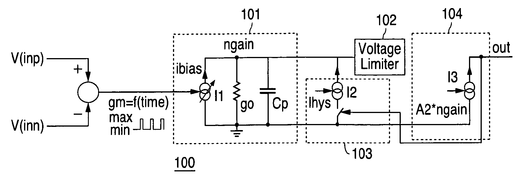
[0015]FIG. 1 depicts an equivalent circuit diagram for a low power integrated circuit comparator with fast propagation delay according to one embodiment of the present invention. Comparator circuit 100 is formed within an integrated circuit device and includes a differential input pair V(inp) and V(inn) producing a pulsed trans-conductance gm received as an input by a first gain stage 101. The pulse input changes the bias current Ibias from the current source I1, changing the bias current of the whole comparator 100.

[0016]The first gain stage 101 includes an output resistance go and output cap...


PUM


Abstract

A direct relationship exists between an integrated comparator's propagation delay and the input differential pair's bias current and overdrive voltage. A new method using a pulsed bias scheme for the input differential pair improves propagation delay by more than one order of magnitude without increasing significantly the average quiescent current, as long as the pulse width of the bias current is small relative to the system clock. A voltage limiter optimizes the comparator's transition time and a built-in hysteresis circuit minimizes spurious output transitions whenever the pulsed bias current pulse changes state. The bias current pulse and sampling of the comparator occur in predefined relation to the system clock.

Description

TECHNICAL FIELD OF THE INVENTION[0001]The present invention is directed, in general, to integrated circuit comparators and, more specifically, to reducing propagation delay in integrated circuit comparators.BACKGROUND OF THE INVENTION[0002]As illustrated in the equivalent circuit diagram depicted in FIG. 4, integrated circuit comparators typically include: a bias system generating a defined current bias to each transistor; an input differential pair—either complementary metal oxide semiconductor (CMOS) or bipolar junction transistors—that, for a given overdrive voltage V(ov)=(V(inp)−V(inn)) generate a differential current given by I(ov)=gm*V(ov), where gm is the transconductance of the input differential pair at the steady-state operating point V(ov)=0 volts (V); a gain stage node ngain converting the current I(ov) to (in the CMOS case) a voltage gain and having a transition speed depending on the overdrive current I(ov) available, the voltage excursion required between the high and...

Claims


Application Information

Patent Timeline
Patent Type & Authority Patents(United States)
IPC IPC(8): H03K5/22
CPCH03K5/2481H03K19/0016H03K5/249
Inventor GUERRERO MERCADO, FRANCISCO JAVIER
Owner NAT SEMICON CORP
Why Eureka
Try Eureka