Display, drive circuit of display, and method of driving display

a drive circuit and display technology, applied in the field of display, can solve problems such as troublesome image display, insufficient sck, etc., and achieve the effects of reducing power consumption, reducing the pulse width of the source shift clock signal, and simplifying circuit design

Inactive Publication Date: 2011-09-27
SHARP KK
View PDF8 Cites 0 Cited by
  • Summary
  • Abstract
  • Description
  • Claims
  • Application Information

AI Technical Summary

Benefits of technology

[0028]According to the first aspect of the present invention, a pulse width of a source shift clock signal to be outputted from the display control circuit is made smaller during a period of time which is immediately before a pulse of a source start pulse signal is outputted. By this, a hold period that is not sufficiently secured in conventional cases is sufficiently secured immediately before the source start pulse signal rises. Hence, without increasing the frequency of a source clock signal or increasing circuit scale, in the video signal line drive circuit, sampling of a video signal can be normally started in each horizontal scanning period. By this, when there is a change in the design of a panel of a display, or the like, a further reduction in power consumption or further simplification of circuit design over conventional cases is made possible.
[0029]According to the second aspect of the present invention, during a period of time which is immediately before a pulse of a source start pulse signal is outputted, by changing a duty ratio of a source shift clock signal to be outputted from the display control circuit, a pulse width of the source shift clock signal is made smaller. By this, a hold period that is not sufficiently secured in conventional cases is sufficiently secured immediately before the source start pulse signal rises and a setup period is secured immediately after the source start pulse signal rises. Accordingly, in the video signal line drive circuit, sampling of a video signal can be normally and more certainly started in each horizontal scanning period.
[0030]According to the third aspect of the present invention, in the source shift clock signal generating circuit, a pulse width of a source shift clock signal is made smaller based on a source shift clock modification command signal to be outputted from the source start pulse signal generating circuit. By this, a pulse width of the source shift clock signal can be easily made smaller only immediately before a source start pulse signal rises.
[0031]According to the fourth aspect of the present invention, the output of a pulse of a source shift clock signal is stopped during a period of time which is immediately before a pulse of a source start pulse signal is outputted. By this, a hold period that is not sufficiently secured in conventional cases is sufficiently secured immediately before the source start pulse signal rises. Hence, without increasing the frequency of a source clock signal or increasing circuit scale, in the video signal line drive circuit, sampling of a video signal can be normally started in each horizontal scanning period. By this, when there is a change in the design of a panel of a display, or the like, a further reduction in power consumption or further simplification of circuit design over conventional cases is made possible.
[0032]According to the fifth aspect of the present invention, in the source shift clock signal generating circuit, the output of a pulse of a source shift clock signal is stopped based on a source shift clock modification command signal to be outputted from the source start pulse signal generating circuit. By this, the output of a pulse of the source shift clock signal can be easily stopped only immediately before a source start pulse rises.
[0033]According to the sixth aspect of the present invention, when there is a change in the design of a panel, or the like, a display is implemented which is capable of achieving a further reduction in power consumption or further simplification of circuit design over conventional cases.

Problems solved by technology

Hence, when a source shift clock signal SCK and a source start pulse signal SSP are generated without setting a hold period in the above-described manner, the delay of the source start pulse signal SSP relative to the source shift clock signal SCK may not be sufficiently large and thus trouble may occur in image display.

Method used


Image

  • Display, drive circuit of display, and method of driving display
  • Display, drive circuit of display, and method of driving display
  • Display, drive circuit of display, and method of driving display

Examples


Embodiment Construction

[0060]An embodiment of the present invention will be described below with reference to the accompanying drawings.

[0061]

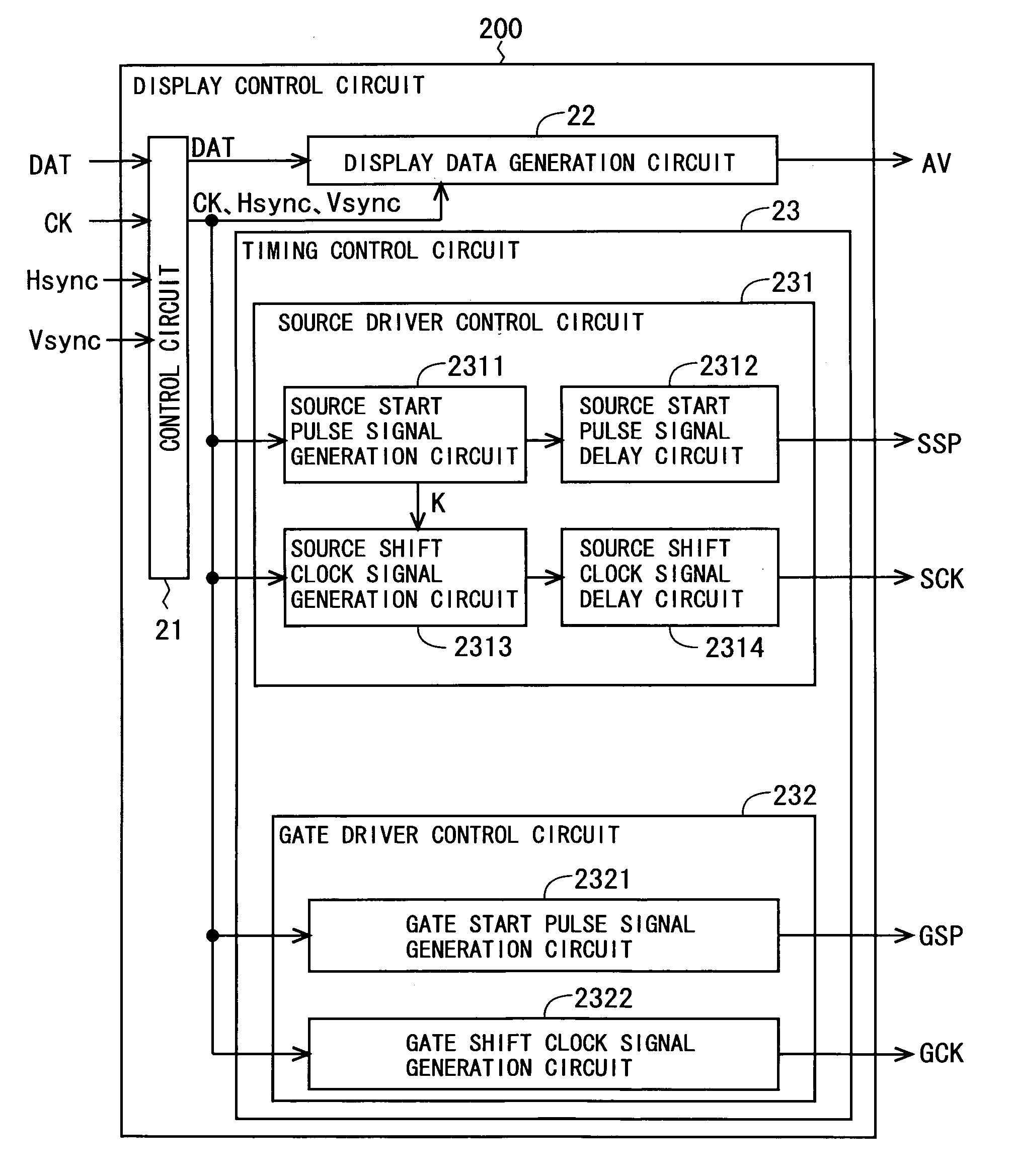
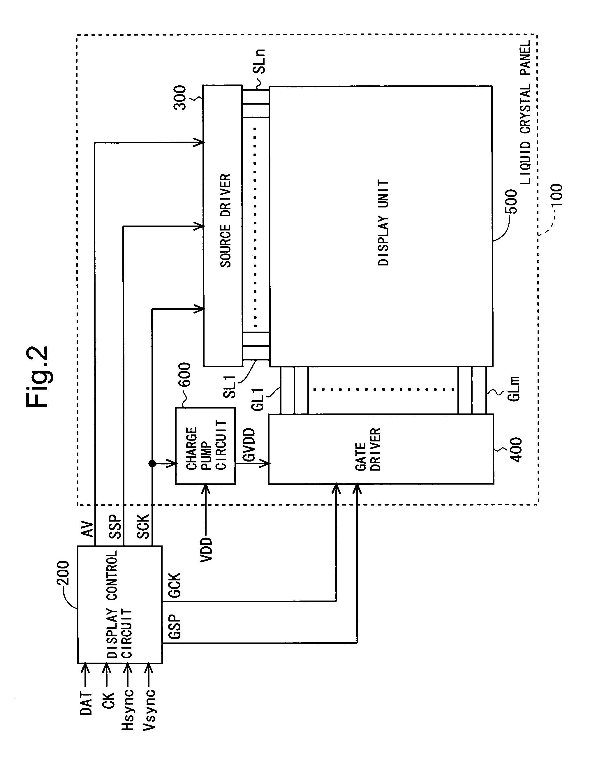
[0062]FIG. 2 is a block diagram showing the overall configuration of an active matrix-type liquid crystal display according to an embodiment of the present invention. The liquid crystal display has a liquid crystal panel 100 including a source driver (video signal line drive circuit) 300, a gate driver (scanning signal line drive circuit) 400, a display unit 500, and a charge pump circuit 600; and a display control circuit 200. The display unit 500 includes a plurality of (n) source bus lines (video signal lines) SL1 to SLn; a plurality of (m) gate bus lines (scanning signal lines) GL1 to GLm; and a plurality of (n×m) pixel formation portions respectively provided at intersections of the plurality of source bus lines SL1 to SLn and the plurality of gate bus lines GL1 to GLm. Each pixel formation portion includes a TFT serving as a switching element; a pixel electrod...


PUM


Abstract

The present invention relates to a display that uses a polysilicon liquid crystal panel.An object of the present invention is to sufficiently secure a hold period and a setup period upon a rise of a source start pulse signal (SSP) without increasing power consumption or increasing circuit scale.A display control circuit (200) includes a source start pulse signal generating circuit (2311) that generates a source start pulse signal (SSP); and a source shift clock signal generating circuit (2313) that generates a source shift clock signal (SCK). The source shift clock signal generating circuit (2313) shortens a period during which the source shift clock signal (SCK) is maintained at a high level, only during a period of time which is immediately before the source start pulse signal (SSP) rises in each horizontal scanning period, based on a source shift clock modification command signal (K) to be outputted from the source start pulse signal generating circuit (2311).

Description

TECHNICAL FIELD[0001]The present invention relates to a display, a drive circuit of the display, and a method of driving the display, and more particularly to a display that uses a polysilicon liquid crystal panel such as a CG silicon liquid crystal panel, a drive circuit of the display, and a method of driving the display.BACKGROUND ART[0002]In recent years, a liquid crystal display that adopts a CG (Continuous Grain) silicon liquid crystal panel has been developed. The CG silicon liquid crystal panel refers to a liquid crystal panel that adopts TFTs (Thin Film Transistors) formed of a CG silicon film, as switching elements. In the CG silicon, grain boundaries are arranged regularly, and the CG silicon has a continuous structure at atomic-level. Therefore, in the CG silicon, electrons can move at high speed and thus a driving integrated circuit can be mounted on a substrate of a liquid crystal panel. By this, a reduction in cost and miniaturization of a device due to a reduction in...

Claims


Application Information

Patent Timeline
Patent Type & Authority Patents(United States)
IPC IPC(8): G09G3/36
CPCG09G3/3611G09G3/3688G09G2370/08
Inventor TOMIYOSHI, AKIRA
Owner SHARP KK
Why Eureka
Try Eureka