Display substrate and method of manufacturing the same

a technology of a substrate and a manufacturing method, applied in the field of a substrate, can solve the problems of undesirable short circuit, difficult control of a pattern skew during the etching process, and the inability to deposit a relatively thick metal layer on the glass substrate, etc., and achieve the effect of thin metal wiring and reduced wiring resistan

Active Publication Date: 2015-05-05
SAMSUNG DISPLAY CO LTD
View PDF20 Cites 3 Cited by
  • Summary
  • Abstract
  • Description
  • Claims
  • Application Information

AI Technical Summary

Benefits of technology

[0030]According to the exemplary embodiments, a thick metal wiring includes a first metal layer, and second metal layer directly on the first metal layer, where a first metal layer excluding the second metal layer is a controlling electrode of a switching element, and a second metal layer excluding the first metal layer is an input or output electrode of the switching element, so that a problem due to a processing stress in forming the thick metal wiring may be reduced, and a wiring's resistance may be decreased.

Problems solved by technology

However, there are limitations in depositing the relatively thick metal layer on the glass substrate.
In addition, it is difficult to control a skew of a pattern during an etching process.
For example, it is difficult to control the skew and a taper angle of the metal layer in forming a channel of a thin film transistor (“TFT”) so that the TFT may be undesirably short-circuited.

Method used


Image

  • Display substrate and method of manufacturing the same
  • Display substrate and method of manufacturing the same
  • Display substrate and method of manufacturing the same

Examples


Embodiment Construction

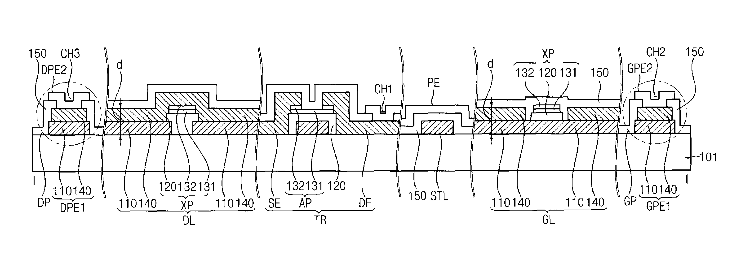
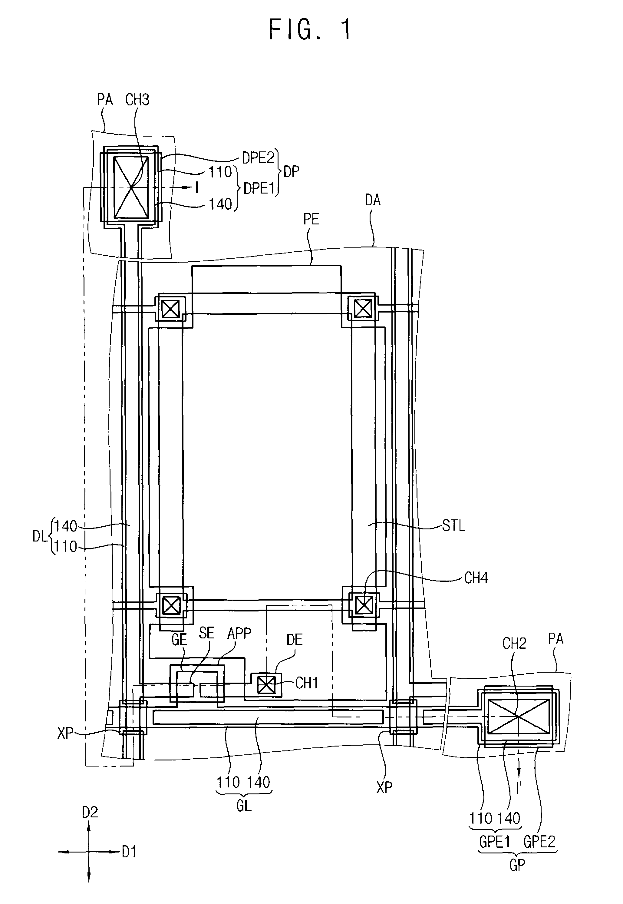
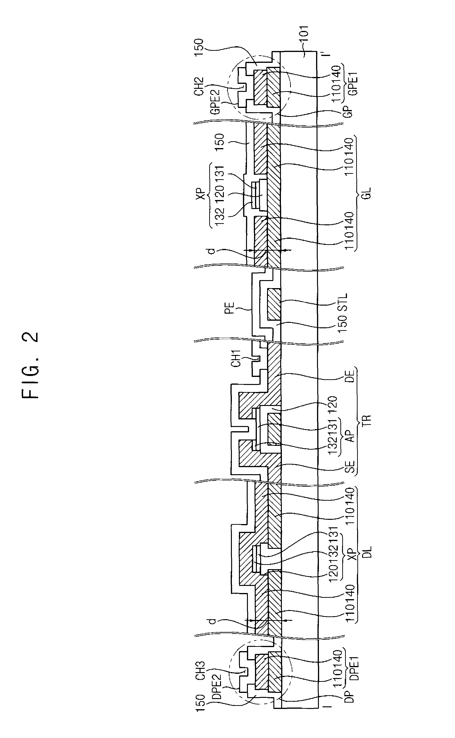
[0037]It will be understood that when an element or layer is referred to as being “on” or “connected to” another element or layer, the element or layer can be directly on or connected to another element or layer or intervening elements or layers. In contrast, when an element is referred to as being “directly on” or “directly connected to” another element or layer, there are no intervening elements or layers present. As used herein, connected may refer to elements being physically and / or electrically connected to each other. Like numbers refer to like elements throughout. As used herein, the term “and / or” includes any and all combinations of one or more of the associated listed items.

[0038]It will be understood that, although the terms first, second, third, etc., may be used herein to describe various elements, components, regions, layers and / or sections, these elements, components, regions, layers and / or sections should not be limited by these terms. These terms are only used to dis...


PUM

PropertyMeasurementUnit
thicknessaaaaaaaaaa
transparentaaaaaaaaaa
total thicknessaaaaaaaaaa

Abstract

A display substrate includes a base substrate, a switching element, a gate line, a data line and a pixel electrode. Each of the gate line and the data line includes a first metal layer, and a second metal layer directly on the first metal layer. The switching element is on the base substrate, and includes a control electrode and an input electrode or an output electrode. The control electrode includes the first metal layer and excludes the second metal layer, and extends from the gate line. The input electrode or the output electrode includes a second metal layer and excludes the first metal layer. The input electrode extends from the data line. The pixel electrode is electrically connected to the output electrode of the switching element through a first contact hole, and includes a transparent conductive layer.

Description

CROSS REFERENCE TO RELATED APPLICATION[0001]This application claims priority to Korean Patent Application No. 10-2011-0111741, filed on Oct. 31, 2011, and all the benefits accruing therefrom under 35 U.S.C. §119, the contents of which are incorporated herein by reference in their entireties.BACKGROUND OF THE INVENTION[0002]1. Field of the Invention[0003]Exemplary embodiments of the invention relate to a display substrate and a method of manufacturing the display substrate. More particularly, exemplary embodiments of the invention relate to a display substrate for forming a metal wiring having a low resistance and a method of manufacturing the display substrate.[0004]2. Description of the Related Art[0005]A liquid crystal display (“LCD”) apparatus includes a thin-film transistor (“TFT”) substrate, a color filter substrate combined with the TFT substrate, and a liquid crystal layer disposed between the TFT substrate and the color filter substrate. The TFT substrate includes a wiring, ...

Claims


Application Information

Patent Timeline
Patent Type & Authority Patents(United States)
IPC IPC(8): G02F1/136G02F1/1362H01L27/12
CPCH01L27/124G02F1/136286H01L27/1288G02F2001/13629G02F1/1368G02F1/13629
Inventor LEE, JUNG-KYUKHANG, YOON-HOYU, SE-HWANKIM, CHEOL-KYULEE, YONG-SUCHANG, CHONG-SUPPARK, SANG-HOKANG, SU-HYOUNGNA, HYUN-JAESHIN, YOUNG-KI
Owner SAMSUNG DISPLAY CO LTD
Why Eureka
Try Eureka