

Electronic device
a small electronic device and electronic technology, applied in the direction of low noise amplifier, low-noise amplifier, semiconductor/solid-state device details, etc., can solve the problems of inevitably long wiring pattern, insufficient area for forming resonators, and insufficient wiring pattern to achieve good electric characteristics, prevent the effect of deterioration of electric characteristics
- Summary
- Abstract
- Description
- Claims
- Application Information
AI Technical Summary
Benefits of technology
Problems solved by technology
Method used
Image

Examples
first embodiment
[0041][1] First Embodiment
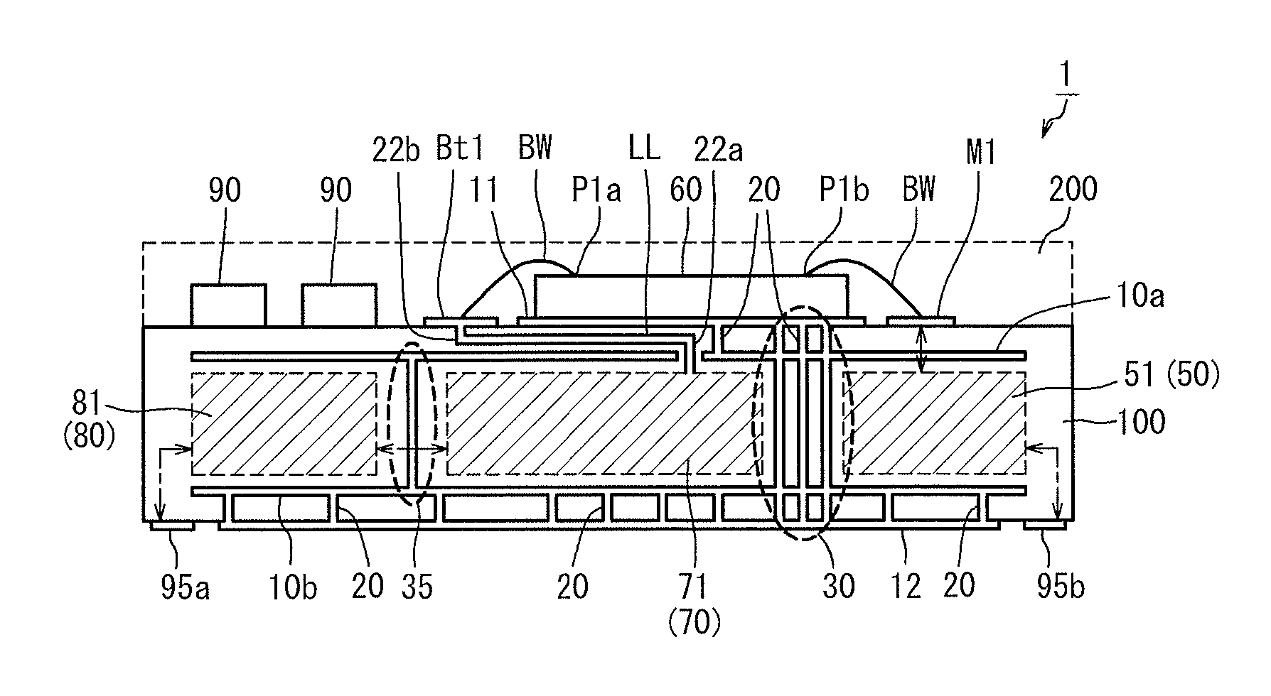
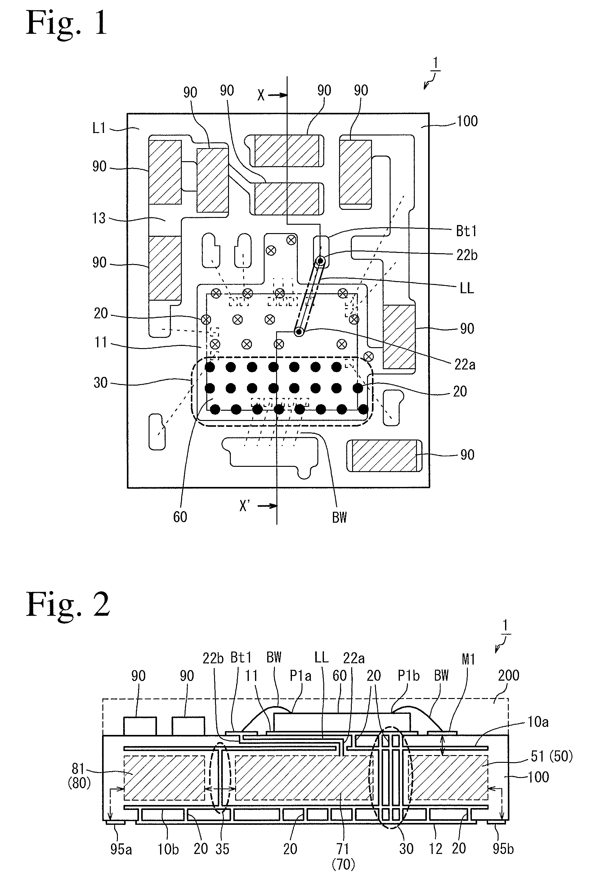
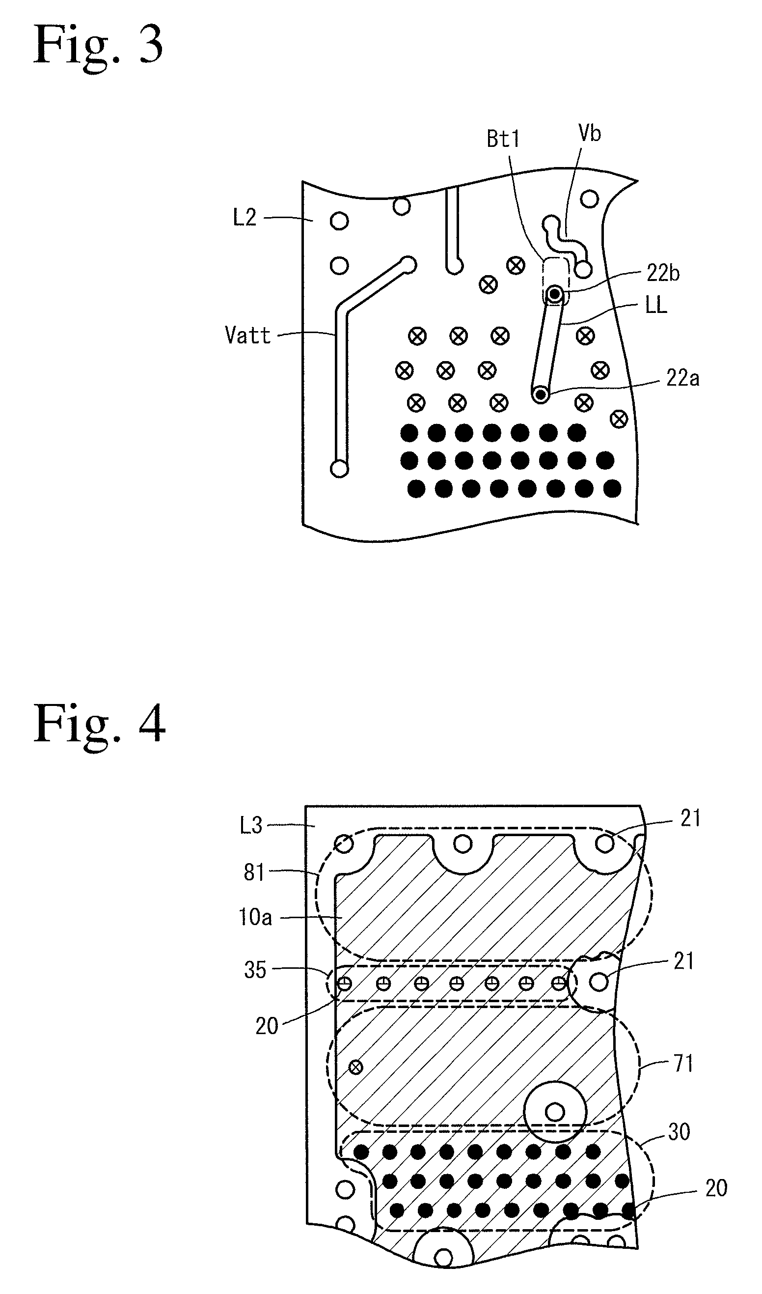
[0042]FIGS. 1-7 show an electronic device 1 according to the first embodiment of the present invention. Although insulator layers L1-L4 shown in FIGS. 1 and 3-5 are indispensable layers, the electronic device 1 of the present invention comprises other insulator layers, too. Accordingly, insulator layers with consecutive reference numerals are not necessarily adjacent to each other. For example, other insulator layers may exist between an insulator layer L3 shown in FIG. 4 and an insulator layer L4 shown in FIG. 5.
[0043]This electronic device 1 comprises a laminate 100 comprising pluralities of insulator layers each provided with conductor patterns, and an amplifier-constituting semiconductor device 60 mounted to a mounting electrode 11 on an upper surface of the laminate 100,[0044]a first ground electrode 10a being formed on an insulator layer near an upper surface of the laminate 100;[0045]a second ground electrode 10b being formed on an insulator layer ne...
second embodiment
[0062][2] Second Embodiment
[0063]FIGS. 8-12 show an electronic device 1 according to the second embodiment of the present invention. This electronic device 1 is used in a high-frequency transmission / reception circuit in a wireless communications apparatus for wireless LAN, comprising pluralities of filters and baluns, and a high-frequency amplifier, a low-noise amplifier and a high-frequency switch mounted on a laminate.
[0064]FIG. 9 shows an equivalent circuit of the electronic device 1. An antenna port ANT is connected via a matching circuit 45 to a single-pole double-throw (SPDT), high-frequency switch 40, to which a transmission signal path and a receiving signal path are connected, a balun 80, a filter 70, a high-frequency amplifier 60, a matching circuit 50 and a filter 54 being disposed in the transmission signal path, and a balun 82, a filter 72, a low-noise amplifier 61 and a filter 52 being disposed in the receiving signal path. Semiconductor devices constituting the high-f...
PUM
 Abstract
Description
Claims
Application Information