

Semiconductor device having vertical channel, resistive memory device including the same, and method of manufacturing the same
a technology of resistive memory and semiconductors, applied in the direction of semiconductor devices, basic electric elements, electrical appliances, etc., can solve the problems that the study of existing electronic charge-controlled devices may encounter limitations
- Summary
- Abstract
- Description
- Claims
- Application Information
AI Technical Summary
Benefits of technology
Problems solved by technology
Method used
Image

Examples
Embodiment Construction
”.
BRIEF DESCRIPTION OF THE DRAWINGS
[0016]Embodiments will be more clearly understood from the following detailed description taken in conjunction with accompanying drawings, in which:
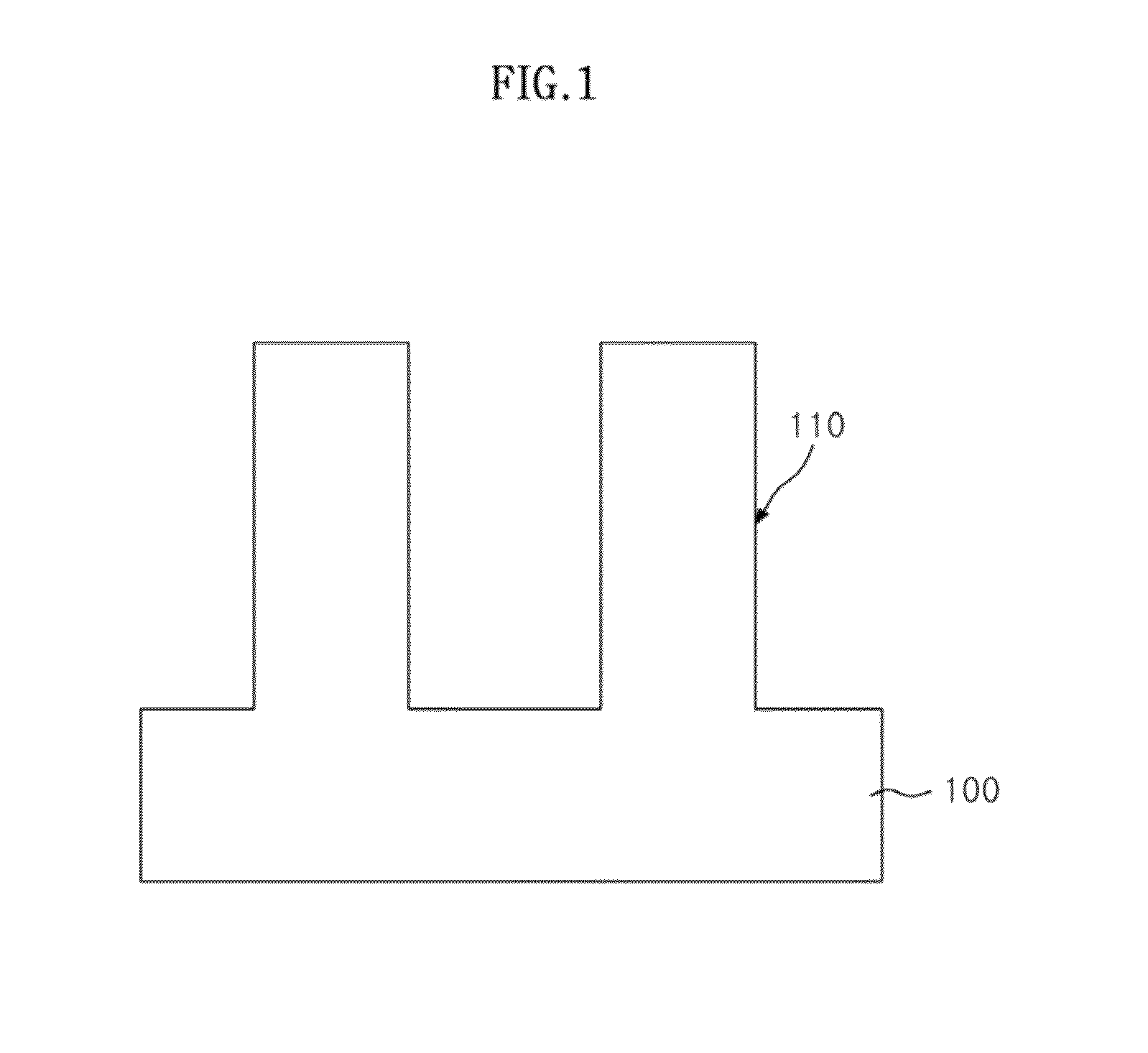
[0017]FIG. 1 is cross-sectional view illustrating a method of manufacturing a semiconductor device having a vertical channel according to an embodiment;
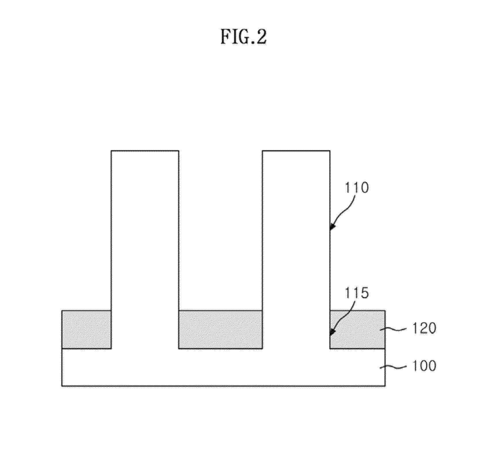
[0018]FIG. 2 is cross-sectional view illustrating a method of manufacturing a semiconductor device having a vertical channel according to an embodiment;
[0019]FIG. 3 is cross-sectional view illustrating a method of manufacturing a semiconductor device having a vertical channel according to an embodiment;
[0020]FIG. 4 is cross-sectional view illustrating a method of manufacturing a semiconductor device having a vertical channel according to an embodiment;
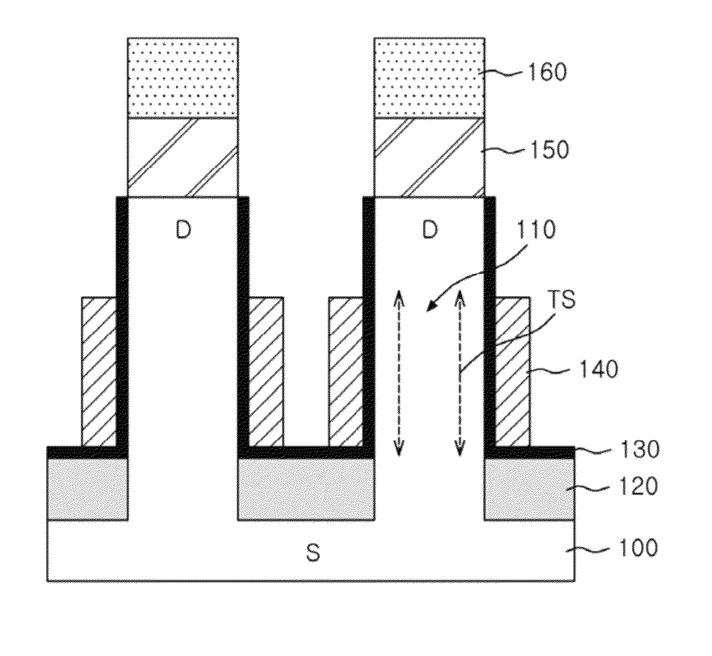
[0021]FIG. 5 is a cross-sectional view illustrating a resistive memory device including a semiconductor device having a vertical channel according to an embodiment.
DETAILED DESCRIPTION
[0022]Hereinafter exem...
PUM
 Abstract
Description
Claims
Application Information