Conductive film with high transmittance having a number of anti reflection coatings, touch panel using the same and manufacturing method thereof

a technology of anti-reflection coating and conductive film, which is applied in the direction of conductive layers on insulating supports, instruments, coatings, etc., can solve the problems of failure to reach a commercially available transmittance, and achieve the effect of improving the transmittance of the ito film, reducing the refractive index and high refractivity

Inactive Publication Date: 2016-10-11
LG INNOTEK CO LTD
View PDF31 Cites 12 Cited by
  • Summary
  • Abstract
  • Description
  • Claims
  • Application Information

AI Technical Summary

Benefits of technology

[0029]The present invention according to an exemplary embodiment has an advantageous effect in that transmittance of an ITO film can be improved by coating a number of anti reflection (AR) coated films having a high refractivity and lower refractivity on a conductive film, and the present invention according to an exemplary embodiment can be advantageously applied to a touch panel of an ITO film / ITO film combination to obtain a clear image thanks to sufficient transmittance.

Problems solved by technology

However, due to the fact that the transmittance of the ITO film is 85-89% level, a panel structure of a film combination of the ITO film / ITO glass may have a transmittance less than 80% arithmetically, resulting in failure to reach a commercializable transmittance.

Method used


Image

  • Conductive film with high transmittance having a number of anti reflection coatings, touch panel using the same and manufacturing method thereof
  • Conductive film with high transmittance having a number of anti reflection coatings, touch panel using the same and manufacturing method thereof
  • Conductive film with high transmittance having a number of anti reflection coatings, touch panel using the same and manufacturing method thereof

Examples


second exemplary embodiment

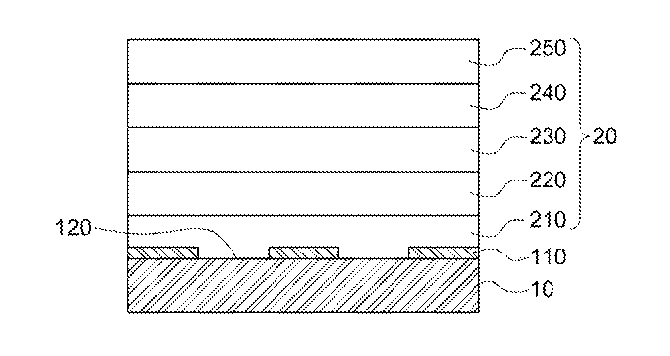
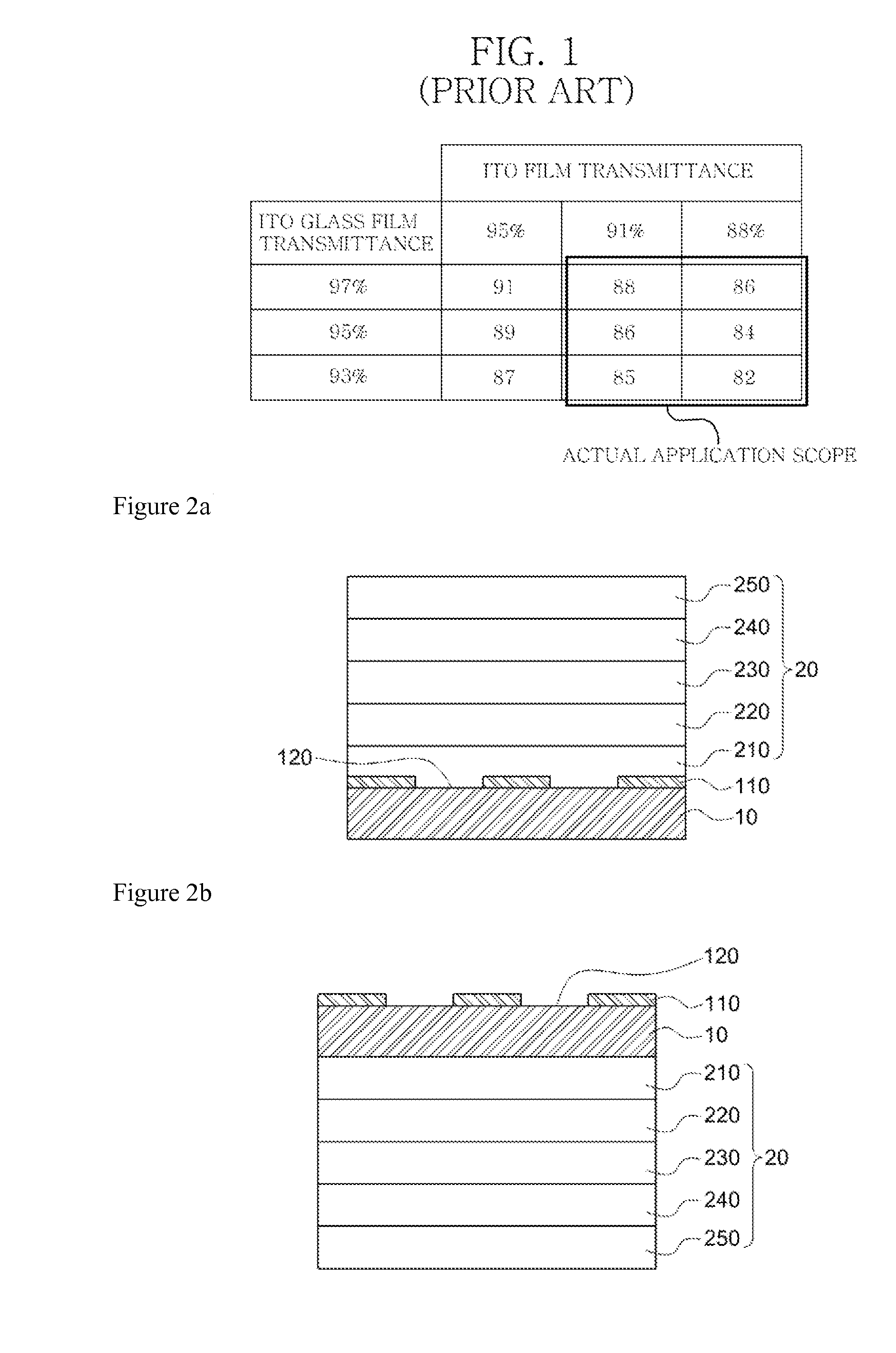
[0058]The second exemplary embodiment of the conductive film with a high transmittance and having a number of anti reflection coated films (20) includes, as shown in FIG. 2b, a conductive film (10) formed with a transparent electrode film pattern (110) and a number of AR films (20) coated in an opposite direction from that of the transparent electrode film pattern (110) on the conductive film (10).

[0059]As in the first exemplary embodiment, the number of anti reflection coated films (20) include a first layer film (210), a second layer film (220), a third layer film (230), a fourth layer film (240) and a fifth layer film (250), each sequentially formed from a surface contacting the conductive film (10) for preventing light reflection, where like reference numerals are used for like and corresponding films of the same layer.

[0060]In second exemplary embodiment, the number of anti reflection coated films (20) are formed on a rear surface of the conductive film (10) formed with the tra...

third exemplary embodiment

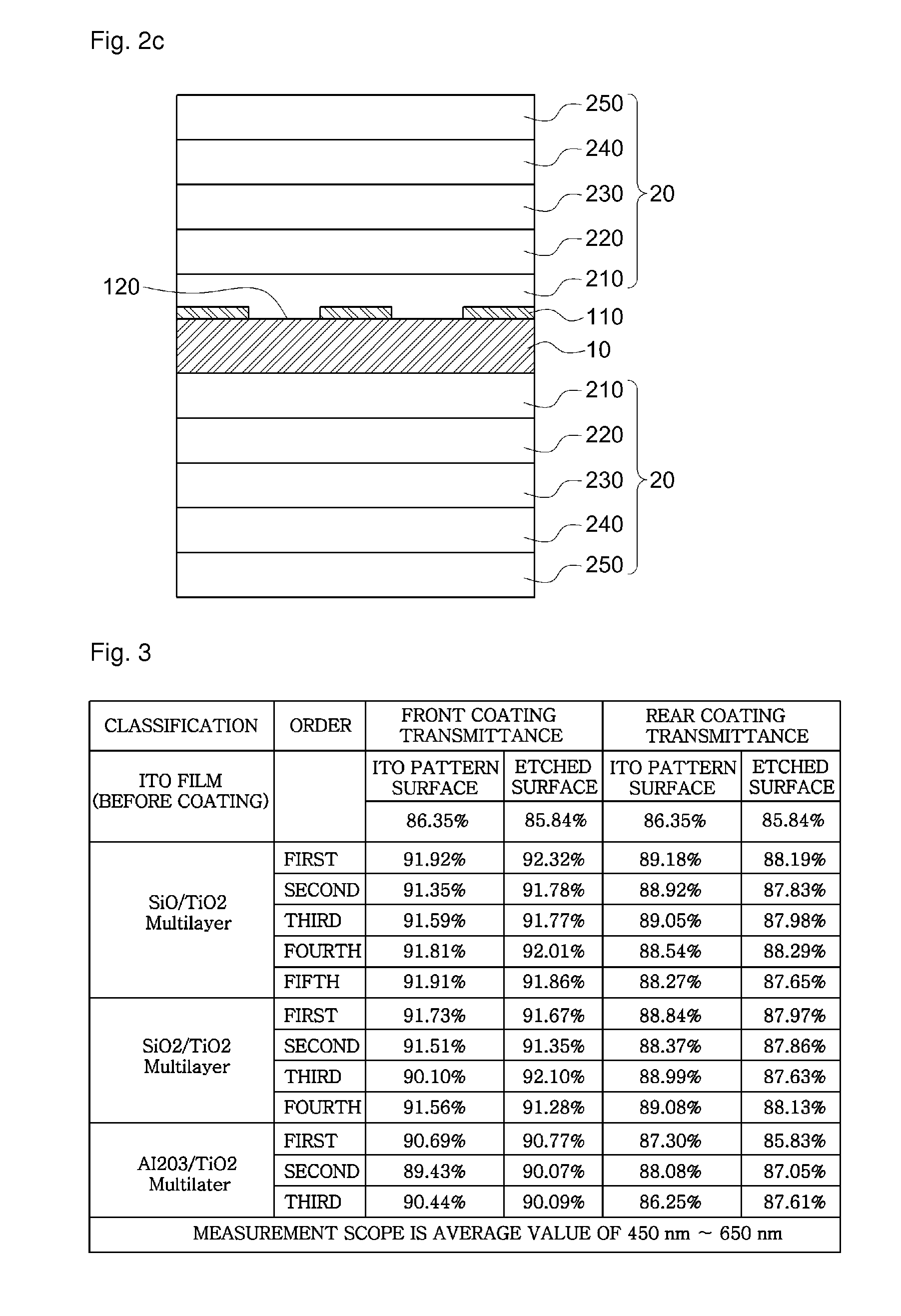
[0061]The third exemplary embodiment of the conductive film with a high transmittance and having a number of anti reflection coated films (20) is a configuration where the number of anti reflection coated films (20) is coated on all the front and rear surfaces to further increase the transmittance and yet to reduce reflectivity, as shown in FIG. 2c.

[0062]In third exemplary embodiment, the number of anti reflection coated films (20) are formed on front and rear surfaces of the conductive film (10) formed with the transparent electrode pattern (110), such that material of film at each layer, the number of layers at each film, and thickness of each film (described later) are same as those of the first and second exemplary embodiments.

experimental examples

[0063]FIG. 3 is a table illustrating an optical transmittance according to each exemplary embodiment of a conductive film with a high transmittance and having a number of anti reflection coated film (20) according to the present invention.

[0064]In the experimental example, the transparent electrode pattern (110) is formed on the conductive film (10) as a test pattern, where the transparent electrode pattern (110) and the etching surface (120) are all provided with a thickness of 3 cm. As illustrated in FIG. 3, it could be noted that a high transmittance (T %) was produced from most of the optical wavelengths of 450 nm˜650 nm under conditions of the following Tables 1 to 6.

[0065]In a case the first layer film (210), which is a base film for the conductive film, is made of silicon monoxide, thickness of each film at each layer of the AR films in the first exemplary embodiment of conductive film with a high transmittance (front coating for the conductive film 10) is as provided in the ...


PUM


Abstract

The present invention relates to a conductive film with high transmittance and having a number of anti reflection (AR) coated films, whereby transmittance of an ITO film can be improved by coating the number of anti reflection (AR) coating having a high refractivity and lower refractivity on the conductive film, and the present invention according to an exemplary embodiment can be advantageously applied to a touch panel of an ITO film / ITO film combination to obtain a clear image due to sufficient transmittance, wherein an exemplary embodiment of the present invention includes a conductive film formed with a transparent electrode pattern, and a number of anti reflection (AR) films formed on at least one surface of the conductive film to prevent optical reflection.

Description

CROSS-REFERENCE TO RELATED APPLICATIONS[0001]This application is the U.S. national stage application of International Patent Application No. PCT / KR2011 / 004538, filed Jun. 22, 2011, which claims priority to Korean Application No. 10-2010-0058999, filed Jun. 22, 2010, the disclosures of each of which are incorporated herein by reference in their entirety.TECHNICAL FIELD[0002]The teachings in accordance with the exemplary embodiments of this invention relate generally to a conductive film with high transmittance. More particularly, the teachings in accordance with the exemplary embodiments of this invention relate to a conductive film formed with a number of anti reflection coatings to reduce reflectivity and yet to increase transmittance, a touch panel using the same, and a manufacturing method thereof.BACKGROUND ART[0003]FIG. 1 is a table showing a transmittance of a touch panel formed with an ITO (Indium Tin Oxide) film and an ITO glass according to prior art. Generally, the touch p...

Claims


Application Information

Patent Timeline
Patent Type & Authority Patents(United States)
IPC IPC(8): H05K1/00H05K1/02H05K3/00G06F3/044G06F3/045
CPCH05K1/0213G06F3/044G06F3/045H05K3/0011G06F3/0443G06F3/0445G06F2203/04103H01B5/14
Inventor NAH, HYUNMIN
Owner LG INNOTEK CO LTD
Why Eureka
Try Eureka