
Slurry for cmp and method of polishing substrate using same
A polishing slurry and substrate technology, applied in the polishing field, can solve the problems of no large particle number analysis, reducing the nitride layer elimination rate, large particle control and other problems
Patent Information
- Authority / Receiving Office
- CN · China
- Current Assignee / Owner
- Publication Date
- 2008-12-24
Smart Images
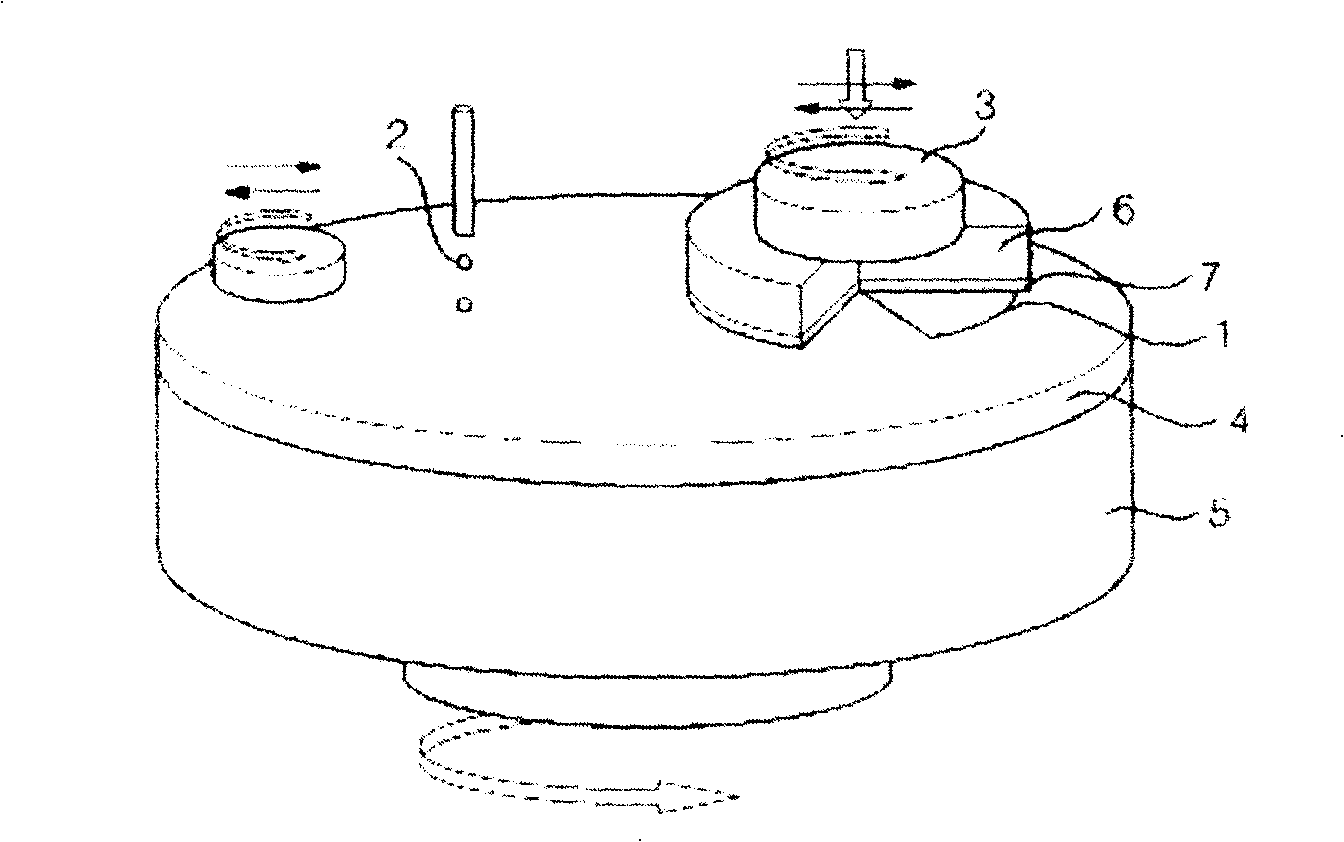
Figure 1 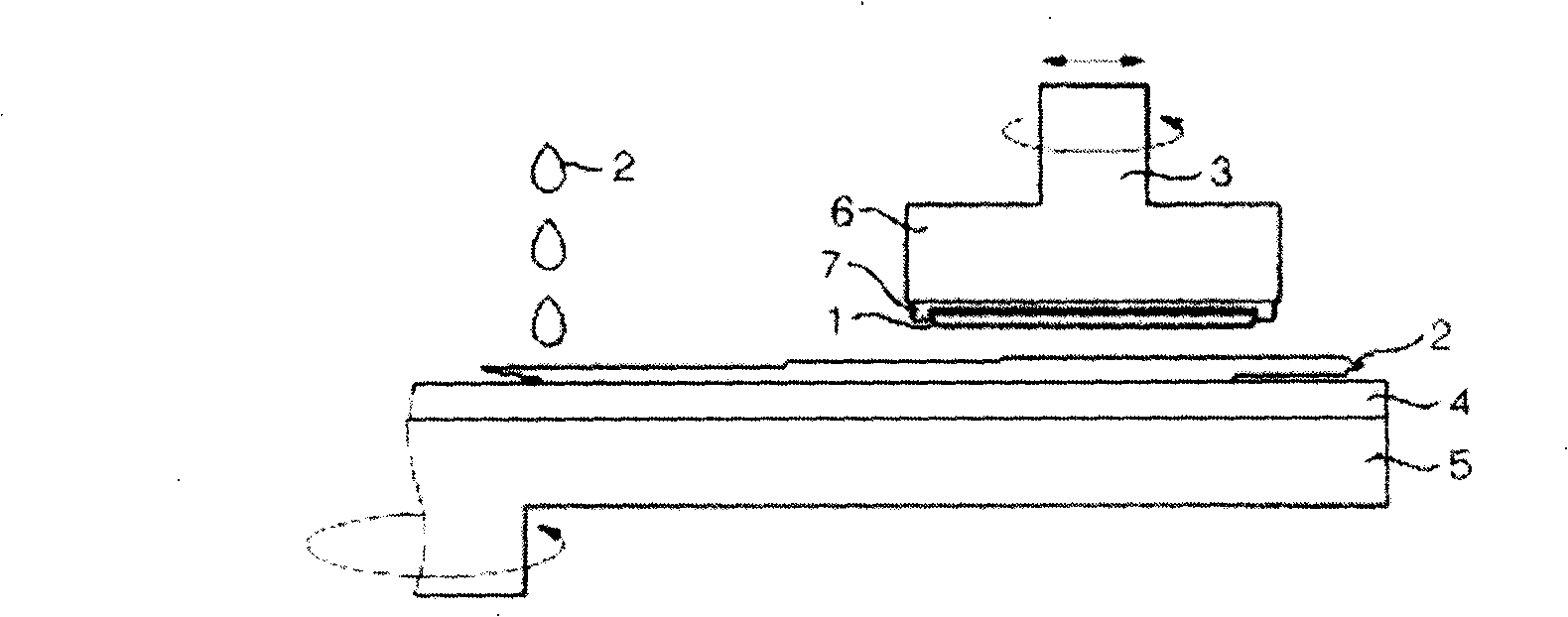
Figure 2 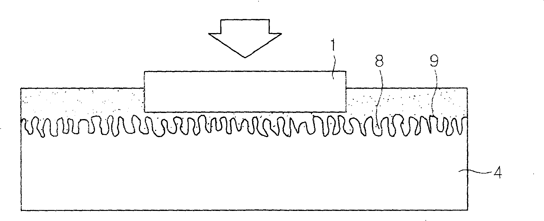
Figure 3
Abstract
Description
technical field
[0001] The present invention relates to a slurry for polishing, especially chemical mechanical polishing (hereinafter referred to as 'CMP'). More specifically, the present invention relates to a method for preparing a high-performance polishing slurry and a method for polishing a substrate. In the manufacturing process of 256 megabytes or higher D-RAM ultra-highly integrated semiconductor silicon wafer (design standard ≤ 0.13 μm), chemical mechanical polishing is carried out with the slurry of the present invention, and the polishing of the oxide layer and the nitride layer The rate is highly selective and scratches are reduced. Background technique
[0002] CMP is a semiconductor processing technology, that is, the polishing slurry is introduced between the clamped wafer and the polishing pad, and mechanical polishing is performed while the chemical corrosion polishes the processed surface. This method has been successfully developed by IBM Corporation of ...
Examples
Embodiment Construction
[0028] The preparation method of the polishing slurry in the present invention and the analysis of the properties of the polishing slurry will be described in detail below. In addition, the present invention will also illustrate the preparation method of polishing slurry using cerium oxide as polishing particles, and the method of using deionized water and anionic polymer as dispersant. Finally, this paper will also give the experimental results of the CMP process, that is, how the oxide film polishing rate and selectivity depend on the process conditions. The present invention may require further improvement in the future, and its scope of application is not limited to the scope discussed herein.
[0029] [Preparation method of ceria polishing slurry]
[0030] The ceria polishing slurry of the present invention comprises ceria powder, deionized water, anionic polymer dispersant and an additive such as a weak acid or a weak base. The preparation method of the polishing slurr...