
coms image sensor and its manufacturing method
A technology of an image sensor and a manufacturing method, which is applied to semiconductor devices, electric solid-state devices, radiation control devices, etc., can solve the problems of white spots in CMOS image sensors, surface damage of semiconductor substrates, etc. white spot effect
Patent Information
- Authority / Receiving Office
- CN · China
- Patent Type
- Patents(China)
- Current Assignee / Owner
- Publication Date
- 2019-06-28
Smart Images
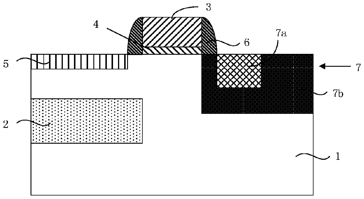
Figure 1 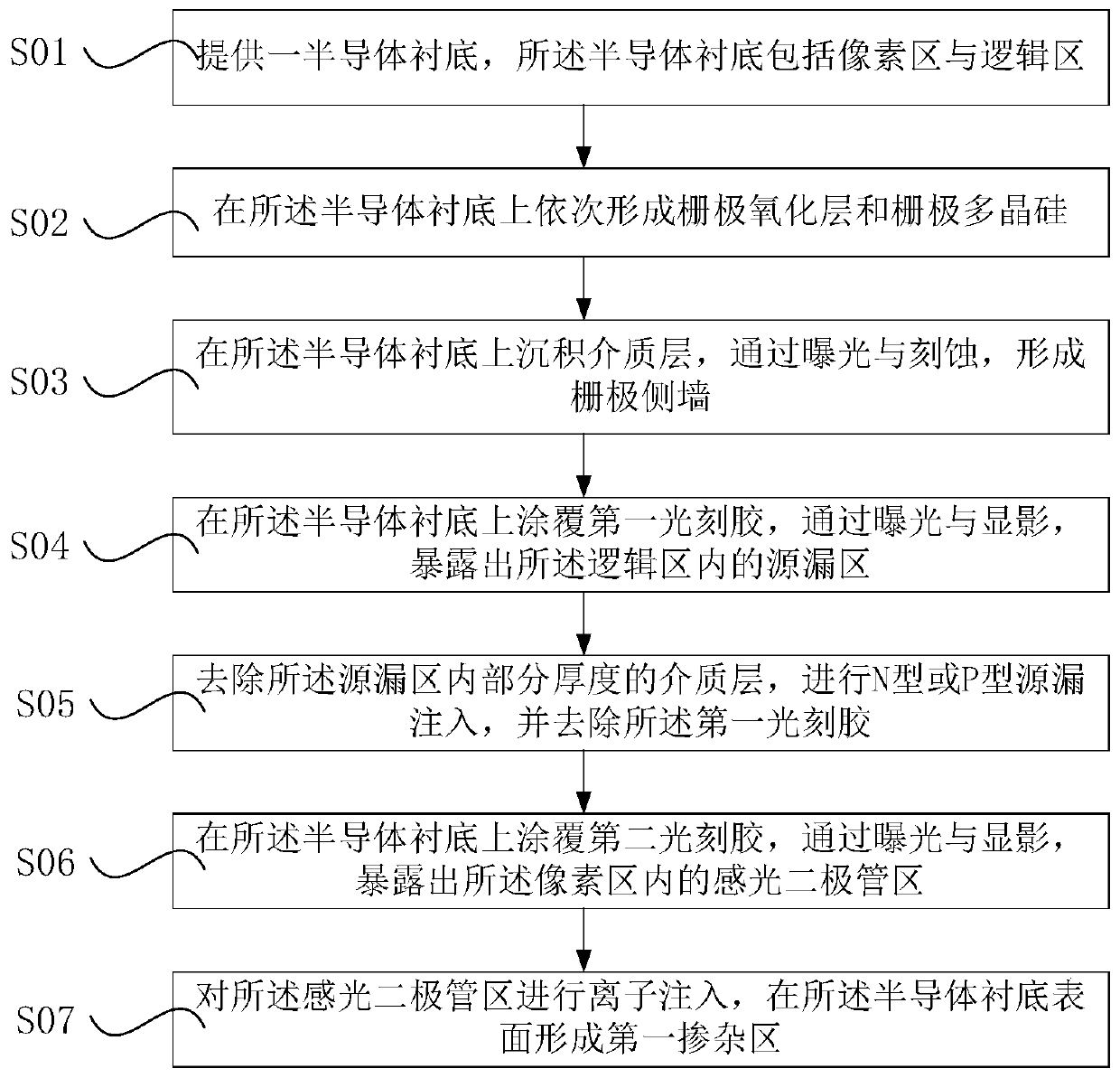
Figure 2 
Figure 3
Abstract
Description
technical field
[0001] The invention relates to the technical field of semiconductors, in particular to a CMOS image sensor and a manufacturing method thereof. Background technique
[0002] Image sensors are an important part of digital cameras. According to the different components, it can be divided into two categories: CCD (Charge Coupled Device, charge-coupled device) and CMOS (Complementary Metal-Oxide Semiconductor, metal oxide semiconductor device). With the continuous development of the manufacturing process of CMOS integrated circuits, especially the design and manufacturing process of CMOS image sensors, CMOS image sensors have gradually replaced CCD image sensors and become the mainstream. Compared with CMOS image sensors, it has the advantages of higher industrial integration and lower power.
[0003] In a CMOS image sensor, a transfer transistor (TX) is used to transfer photogenerated electrons in a photodiode.
[0004] figure 1 A schematic structural diagra...
Examples
Embodiment Construction
[0035] It can be seen from the background art that the CMOS image sensor formed in the prior art causes damage to the surface of the semiconductor substrate due to ion implantation, resulting in white spots. The inventors have conducted research on the above problems and found that after the dielectric layer is removed by sidewall etching, the subsequent ion implantation of the doped layer on the surface of the photodiode will cause damage to the semiconductor substrate on the surface of the photodiode, and the white spots will affect the surface quality of the photodiode. And integrity is very sensitive, damage to the semiconductor substrate can cause white spots in the CMOS image sensor.
[0036] After further research, the inventor proposed a CMOS image sensor and a manufacturing method thereof.
[0037] The CMOS image sensor proposed by the present invention and its manufacturing method will be further described in detail below in conjunction with the accompanying drawings...