

Epoxy resin composition for encapsulating semiconductor device and semiconductor device encapsulated using same
A technology of epoxy resin and composition, which can be used in semiconductor devices, semiconductor/solid-state device parts, electric solid-state devices, etc., and can solve problems such as explosions
Patent Information
- Authority / Receiving Office
- CN · China
- Current Assignee / Owner
- Publication Date
- 2020-08-11
Smart Images
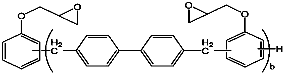
Figure 1 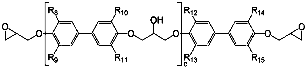
Figure 2 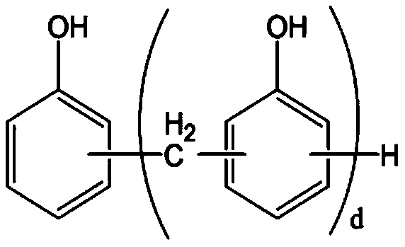
Figure 3
Abstract
Description
technical field
[0001] The present invention relates to an epoxy resin composition for packaging a semiconductor device and a semiconductor device packaged using the epoxy resin composition. Background technique
[0002] In order to protect semiconductor devices from external environments such as moisture or mechanical shocks, semiconductor devices are generally encapsulated with epoxy resin compositions.
[0003] The fields of application of semiconductor devices have been diversified, and in recent years, the demand for semiconductor devices requiring a high relative permittivity is rapidly increasing in this field.
[0004] Among various biometric chips used in mobile devices or automobiles, the application of fingerprint biometric chips has rapidly spread in this field due to its low cost and identification convenience, and the research on capacitive fingerprint identification methods is also developing rapidly. The capacitive fingerprint recognition method is a method ...
Examples
Embodiment 1 to 7 and comparative Embodiment 1 to 4
[0175] The above-mentioned components were weighed in the amounts listed in Table 2, and uniformly mixed using a Henschel mixer, thereby preparing a primary composition in powder form. Then, the primary composition was subjected to melt-kneading at 120° C. for 30 minutes using a continuous kneader, and then cooled and pulverized at 10-15° C., thereby preparing an epoxy resin composition for encapsulating a semiconductor device.
[0176] [Table 1]
[0177]
[0178] (In Table 1, the content of (H) refers to the weight percent (wt%) relative to 100wt% of the inorganic filler).
[0179] The following properties of each epoxy resin composition for encapsulating a semiconductor device prepared in Examples and Comparative Examples were evaluated by the following methods. The results are shown in Table 3.
[0180] property evaluation
[0181] (1) Spiral flow (inch): The epoxy resin composition is injected into the mold for use with a low-pressure transfer molding machine at a mo...