
Scanning Probe Microscope and Surface Shape Measuring Method Using Same
Patent Information
- Authority / Receiving Office
- US · United States
- Current Assignee / Owner
- Publication Date
- 2013-08-15
Smart Images
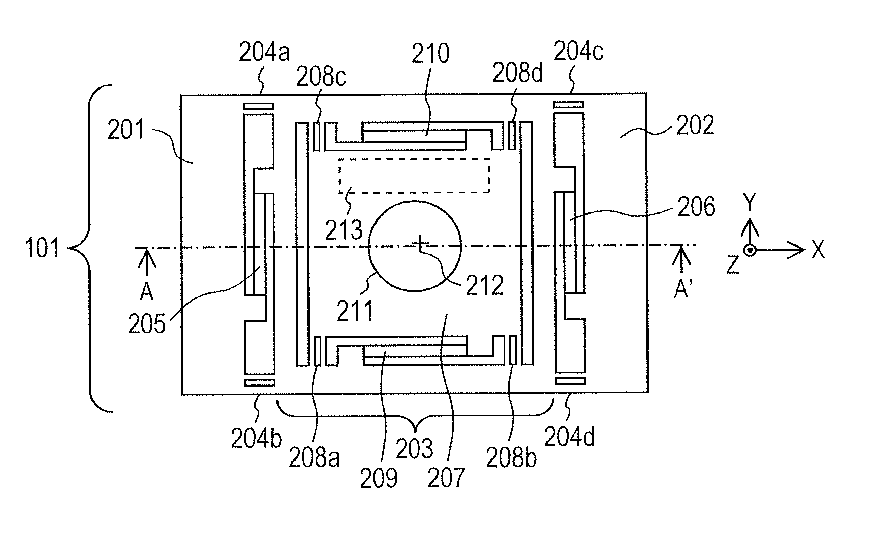
Figure 1 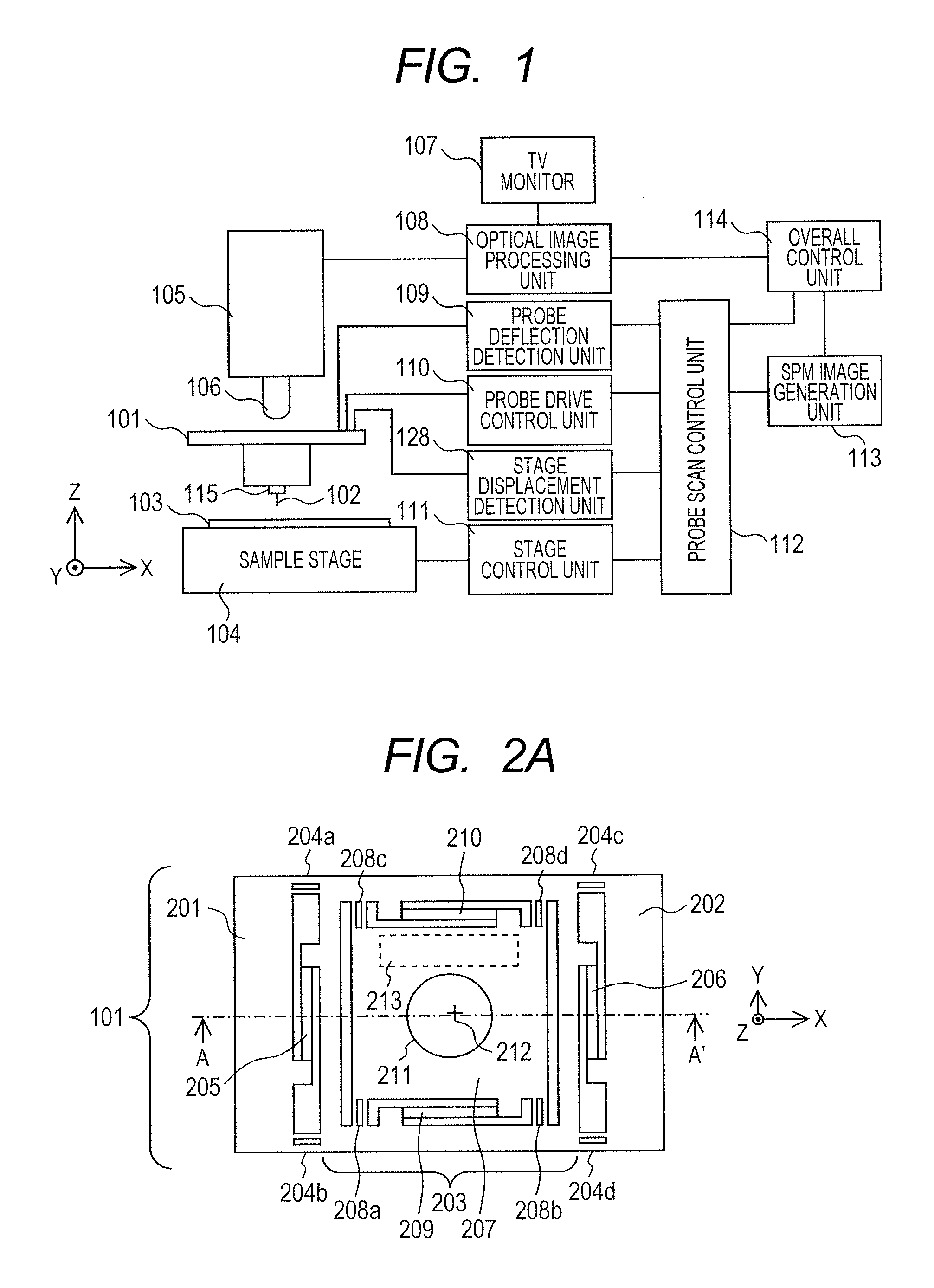
Figure 2 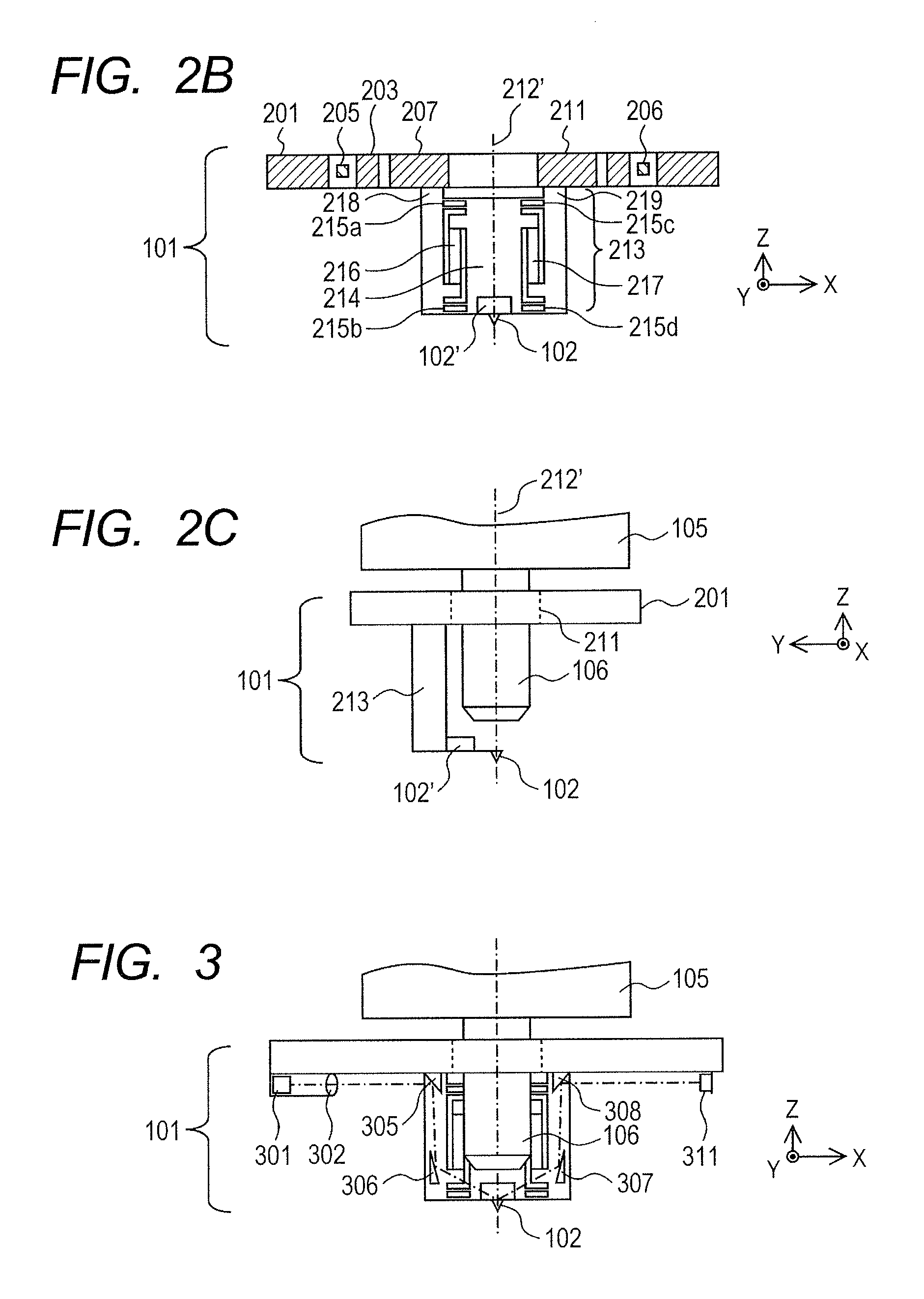
Figure 3
Abstract
Description
TECHNICAL FIELD
[0001] The present invention relates to a scanning probe microscope for high-accuracy measurement of a sample shape, and a surface shape measuring method of the sample using the same.BACKGROUND
[0002] With the miniaturizing trend of circuit patterns in progress associated with high integration of the semiconductor circuit, inspection measurement technique and failure analysis technique for the semiconductor manufacturing process has been increasingly recognized as important. Increase in the recording density of the hard disk device has placed more importance on the miniature structure or planarity of the pole part of the record / reproduction head, surface roughness of the recording medium, and measurement of a three-dimensional shape of stripe-like or dot-like structure of magnetism for further improving the recording density. The scanning probe microscope (hereinafter referred to as SPM: Scanning Probe Microscope) optimal for such usage has been widely known as an approa...
Examples
Embodiment Construction
[0069]As a first embodiment of the present invention, a structure of the SPM as a base of the invention will be described referring to FIGS. 1 to 3. Referring to FIG. 1, a reference numeral 103 denotes a measuring sample, 104 denotes a sample stage which holds the sample 103 through vacuum suction so as to be moved in X-, Y-, and Z-directions, and a rotating direction in an XY-plane. Operations of the sample stage are controlled by a stage control unit 111. A probe 102 is held by a probe drive mechanism 101 via a probe holder 115.
[0070]The probe drive mechanism 101 accurately positions the probe 102 above the sample 103 in the X-, Y- and Z-directions. The probe 102 is formed of a silicon material, and has a tip processed through etching or focused ion beams to have a diameter of 10 nanometers or less. Alternatively, it may have the tip provided with a carbon nanotube with the diameter of approximately 10 nm. The probe 102 includes a cantilever and the probe formed on the distal end ...